
The semiconductor industry built its dominance on a single assumption: that shrinking transistors onto ever-larger monolithic dies would deliver the performance gains that compute-hungry applications demand. That assumption held for decades. It is no longer holding. The physical and economic constraints of monolithic chip design have pushed chiplet architecture from an experimental approach into the mainstream path forward for AI compute. The shift is not gradual. It is structural, and the infrastructure implications for AI data centers are significant.
What Chiplet Architecture Actually Means
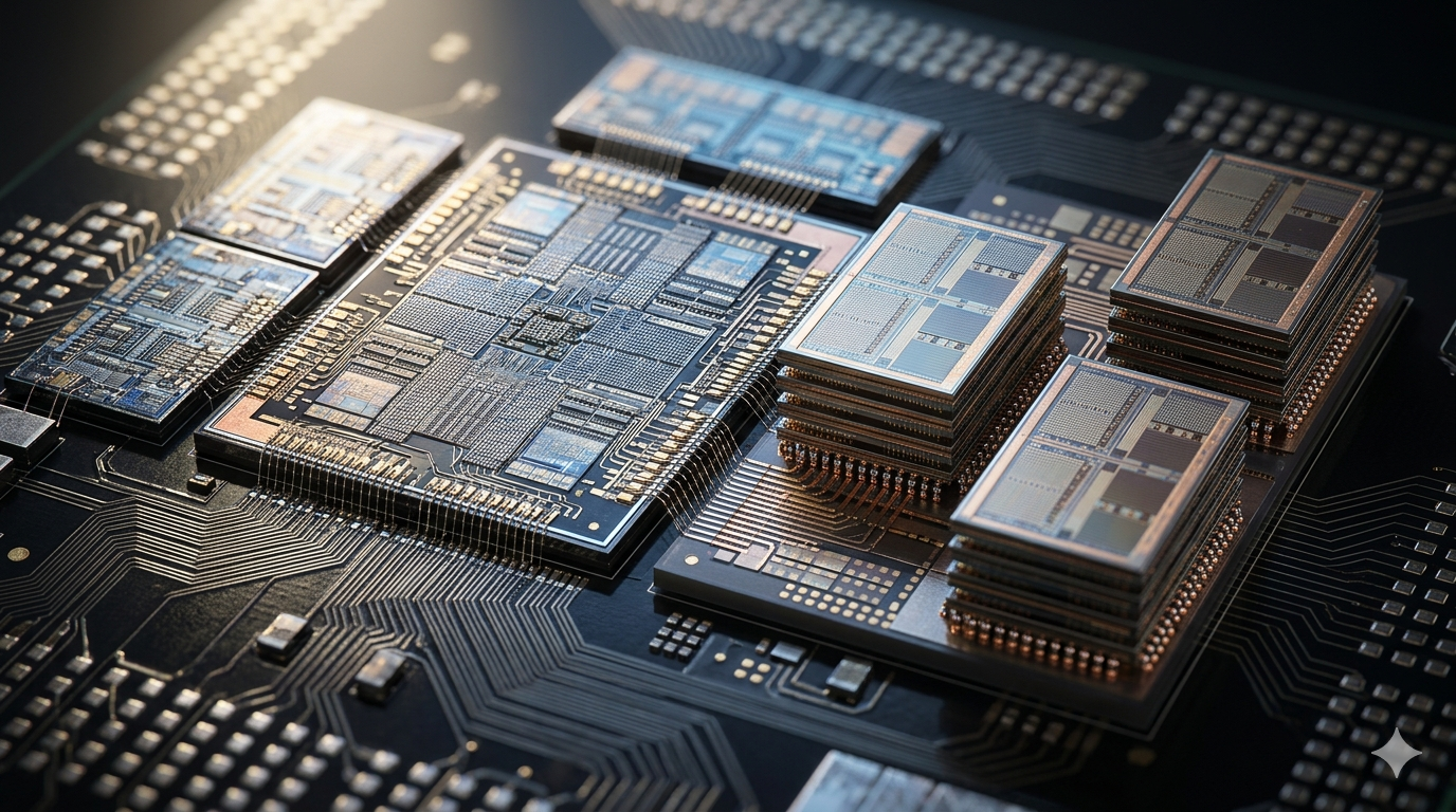
A chiplet is a small, modular semiconductor die designed to connect with other dies to form a complete processor. Instead of manufacturing everything on a single large piece of silicon, chiplet-based designs assemble multiple specialized dies into one package. Each die handles a specific function, whether compute, memory, input/output, or networking, and connects to the others through high-bandwidth interconnects. The result is a processor that performs like a monolithic chip but gets manufactured as a collection of smaller, more manageable components.
The manufacturing advantage of this approach is substantial. Larger dies carry higher defect rates because any flaw anywhere on the silicon renders the entire chip unusable. Smaller dies have lower defect rates and higher yields. A chiplet design can also mix dies manufactured at different process nodes within the same package. A compute die might use the most advanced node available while a less performance-sensitive input/output die uses a cheaper, older process. This flexibility reduces cost without sacrificing performance where it matters most.
Why Monolithic Scaling Hit Its Limits for AI
AI workloads exposed the limits of monolithic chip design faster than any other application category. Training large AI models requires simultaneous access to vast amounts of memory and compute bandwidth. Monolithic designs struggle to deliver both within the thermal and power constraints of a single die at advanced process nodes. As transistor density increases, so does heat generation per unit area. Managing that heat while maintaining performance becomes increasingly difficult and expensive at the die sizes that AI compute demands.
The economics compounded the physics problem. Manufacturing large monolithic dies at leading-edge nodes is extraordinarily expensive. Yields fall as die size grows. The cost per functional unit of compute rises in ways that chiplet designs can avoid by keeping individual dies small and combining them into larger systems. For AI infrastructure operators who buy compute at scale, the cost trajectory of monolithic designs relative to chiplet alternatives has become a meaningful factor in procurement decisions. The AI chip market is reorganizing around this reality.
How the Major Players Are Moving
Nvidia, AMD, and Intel have all moved toward chiplet-based designs for their highest-performance AI compute products. AMD’s approach through its 3D V-Cache technology and multi-die packaging demonstrated early that chiplet designs could match or exceed monolithic performance in real workloads. Intel’s Foveros packaging technology takes the same logic further, stacking dies vertically to reduce interconnect distance and improve bandwidth. Nvidia’s packaging strategies for its Hopper and Blackwell architectures incorporate chiplet-adjacent approaches that allow the company to scale compute and memory bandwidth independently.
The strategic implication of this convergence is significant. When the three dominant players in AI compute all move toward chiplet architectures simultaneously, the ecosystem around them follows. Memory suppliers, packaging specialists, interconnect standard bodies, and software toolchains all adapt to the new architectural reality. That ecosystem alignment is what converts a design trend into a default architecture. It is happening now, and the pace is accelerating as AI hardware demand pulls investment into chiplet-enabling technologies across the supply chain.
What This Means for AI Infrastructure Operators
The shift to chiplet architecture changes how AI infrastructure operators think about hardware procurement, facility design, and upgrade cycles. Chiplet-based processors can be updated more granularly than monolithic designs. A compute die can be refreshed at a new process node while the memory and input/output dies remain unchanged. This modularity has the potential to extend the useful life of AI infrastructure investments by allowing partial upgrades rather than full system replacements.
The thermal and power implications of chiplet architecture also affect facility design. Chiplet packages concentrate heat in ways that differ from monolithic dies. The interconnects between dies generate their own thermal signatures. Facilities designed around direct-to-chip cooling are better positioned to manage these characteristics than air-cooled environments. As chiplet adoption accelerates, the relationship between chip architecture and cooling infrastructure strategy will become tighter. Operators who understand that relationship early will make better facility design decisions than those who treat hardware and infrastructure as independent choices.
The Interconnect Problem That Still Needs Solving
Chiplet architecture introduces a challenge that monolithic designs do not face: the interconnect between dies. Data moving between chiplets must cross a physical boundary that adds latency and consumes power. The performance of a chiplet-based processor depends heavily on how well that interconnect is engineered. Industry standardization efforts like UCIe, the Universal Chiplet Interconnect Express specification, aim to create a common interface that allows chiplets from different manufacturers to connect reliably. Progress on UCIe and similar standards will determine how far chiplet architecture can scale before interconnect limitations become the binding constraint.
For AI compute specifically, the interconnect problem maps directly onto the memory bandwidth problem that limits model training performance. A chiplet design that connects high-bandwidth memory dies to compute dies through a well-engineered interconnect can deliver memory bandwidth that monolithic designs cannot match at equivalent cost and power. That bandwidth advantage is precisely what large AI model training requires. The chiplet designs that solve the interconnect problem most effectively will define the performance ceiling for AI compute over the next several hardware generations. The infrastructure built around those designs will need to be ready for what they demand.


