The semiconductor industry long equated scale with transistor density, pushing monolithic chips toward their physical and economic limits. That model now faces diminishing returns as node advancements slow and costs rise sharply at leading-edge processes. Chiplets introduce a different path, breaking large chips into smaller, purpose-built components that integrate within a single package. This shift allows performance to scale through smarter composition rather than brute-force miniaturization. Designers can now combine specialized dies, optimize them independently, and assemble systems tailored to specific workloads. The result is a structural change in how compute power gets built, measured, and delivered across modern AI infrastructure.
The semiconductor industry built its foundation on monolithic chip design, where performance scaled through shrinking process nodes and increasing transistor density on a single die. However, physical and economic limits have slowed node advancements, making it harder to extract linear performance gains from traditional scaling methods. Chiplets introduce a structural shift by decomposing large chips into smaller, specialized dies that integrate within a single package. This modular approach allows designers to bypass yield constraints associated with large monolithic dies while maintaining high aggregate performance. It also reduces the cost per functional unit because smaller dies achieve higher manufacturing yields compared to large, defect-prone wafers. As a result, chiplets redefine scaling by focusing on system-level composition rather than lithographic advancement alone.
This transition changes how performance scaling gets measured, moving away from transistor density toward bandwidth, interconnect efficiency, and heterogeneous integration. Chiplet-based systems enable designers to mix process nodes, allowing critical compute dies to use advanced nodes while less sensitive components rely on mature, cost-efficient nodes. Such flexibility was not possible in monolithic architectures where all components shared the same fabrication process. Chiplets accelerate iteration cycles by enabling reuse of modular components and reducing the need to redesign entire systems for incremental changes. Consequently, the industry no longer depends solely on leading-edge fabs to push performance boundaries.
Packaging Is the New Compute Layer
The architectural implications extend into system design, where chiplets introduce a new abstraction layer between silicon and application workloads. Designers now think in terms of functional partitioning rather than monolithic integration, allowing more precise optimization for specific compute tasks. This model aligns well with AI infrastructure, where workloads demand different compute characteristics across training and inference stages. Chiplets enable tailored architectures that match workload-specific requirements without overprovisioning resources. Therefore, efficiency improves not only at the silicon level but across the entire compute stack. The result is a gradual erosion of the dominance previously held by single-die architectures in high-performance computing.
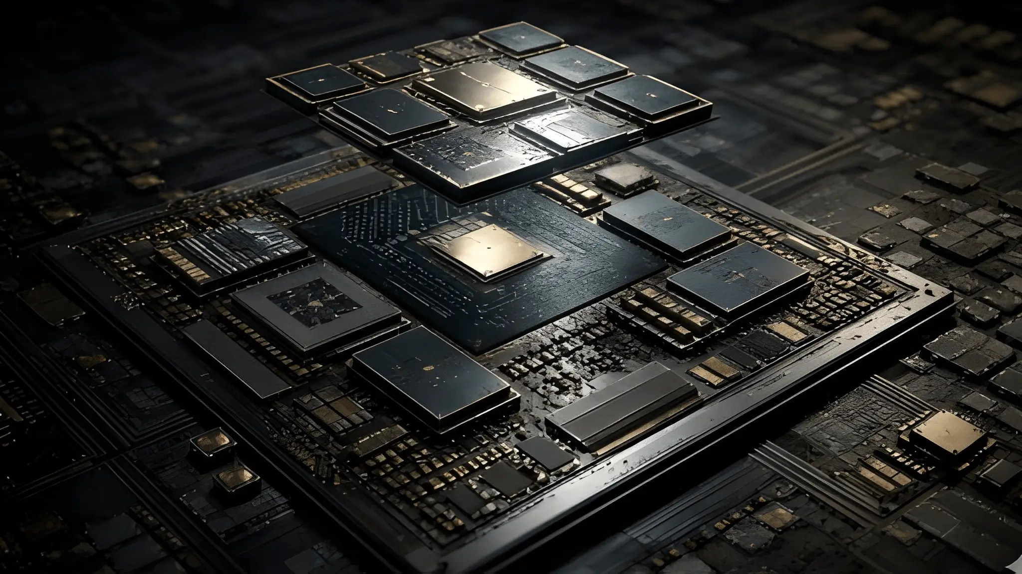
Advanced packaging technologies have evolved into a primary driver of performance in chiplet-based systems, shifting focus from fabrication to integration. Techniques such as 2.5D interposers and 3D stacking allow multiple chiplets to communicate at high bandwidth and low latency within a single package. This configuration effectively turns packaging into an extension of the compute fabric rather than a passive enclosure. High-bandwidth memory integration, enabled through these packaging methods, significantly reduces data movement bottlenecks in AI workloads. The proximity between compute and memory improves throughput while lowering energy consumption per operation. As a result, packaging has become a critical factor influencing achievable system performance alongside compute architecture and process technology.
The rise of packaging-centric performance introduces new constraints that differ from traditional fabrication challenges. Interconnect density, signal integrity, and thermal management now determine how effectively chiplets operate as a unified system. These factors require sophisticated design methodologies that integrate electrical, mechanical, and thermal considerations simultaneously. Packaging technologies such as CoWoS and Foveros illustrate how vertical and horizontal integration strategies can optimize different performance dimensions. However, these approaches also introduce complexity in manufacturing workflows, as multiple dies must align with high precision. Consequently, packaging capacity has emerged as a bottleneck in AI chip production, affecting supply availability and deployment timelines.
The strategic importance of packaging reshapes the semiconductor value chain by elevating the role of outsourced assembly and test providers. Foundries no longer operate as the sole gatekeepers of performance, as packaging expertise becomes equally critical. This shift redistributes competitive advantage toward companies that can orchestrate advanced integration techniques at scale. AI infrastructure providers now evaluate packaging capabilities alongside fabrication nodes when selecting hardware partners. Meanwhile, investments in packaging capacity continue to rise as demand for AI accelerators grows across industries. Therefore, packaging has transitioned from a supporting function into a central pillar of compute architecture.
Custom Silicon Without Owning a Fab
Chiplets enable a new model of semiconductor innovation where companies can design custom silicon without investing in fabrication infrastructure. This model leverages a distributed ecosystem of foundries, IP vendors, and packaging specialists to bring products to market. Cloud providers and startups can now focus on architectural differentiation rather than capital-intensive manufacturing. By combining pre-designed chiplets with custom components, they can create application-specific accelerators tailored to AI workloads. This approach reduces certain barriers to entry such as upfront design cost and development flexibility, while still requiring significant expertise in integration and system validation. As a result, ownership of fabs is no longer the sole determinant of access to advanced silicon capabilities, although leading-edge manufacturing remains concentrated among a few foundries.
The economic implications extend beyond cost reduction, influencing how innovation cycles evolve across the industry. Companies can iterate on individual chiplets independently, reducing development time and enabling faster deployment of new features. This modularity supports rapid experimentation, which is essential in AI environments where workloads and models change frequently. Additionally, it allows firms to source components from multiple vendors, increasing supply chain resilience. However, this flexibility introduces challenges in standardization, as interoperability between chiplets becomes critical for system functionality. Industry initiatives such as the Universal Chiplet Interconnect Express aim to address these concerns by defining common communication protocols.
The emergence of fabless chiplet ecosystems also shifts competitive dynamics toward design expertise and system integration capabilities. Companies that excel in workload-specific optimization gain an advantage over those relying solely on manufacturing scale. This trend aligns with broader shifts in cloud infrastructure, where differentiation increasingly occurs at the software and system level. AI service providers can integrate custom silicon directly into their platforms, optimizing performance for specific applications. Consequently, the boundaries between hardware and software continue to blur, creating new opportunities for vertically integrated solutions. The semiconductor industry thus moves toward a more distributed and collaborative innovation model.
AI Workloads Are Driving Modular Architectures
AI workloads introduce diverse computational requirements that challenge the efficiency of uniform chip architectures. Training large models demands high throughput and memory bandwidth, while inference prioritizes latency and energy efficiency. Chiplets provide a mechanism to address these divergent needs by enabling heterogeneous integration within a single package. Designers can combine compute chiplets, memory modules, and specialized accelerators to create workload-specific configurations. This flexibility allows resources to align more closely with application requirements, which can improve efficiency compared to generalized designs in specific workload scenarios. As AI adoption expands, the need for such tailored architectures continues to grow across industries.
The modular nature of chiplets also supports scalability across different deployment environments, from hyperscale data centers to edge devices. Systems can scale horizontally by adding more chiplets or vertically through advanced stacking techniques. This adaptability allows organizations to optimize infrastructure based on performance, power, and cost constraints. Furthermore, it enables incremental upgrades, where specific components can be replaced without redesigning the entire system. Such flexibility proves valuable in AI ecosystems, where rapid advancements require continuous hardware evolution. Consequently, modular architectures align closely with the dynamic nature of AI workloads.
The integration of diverse components within chiplet-based systems introduces new opportunities for specialization. Designers can incorporate domain-specific accelerators alongside general-purpose compute units to enhance performance for targeted applications. This approach reduces reliance on monolithic GPUs and encourages a more distributed compute model. It also enables better utilization of resources by matching hardware capabilities with workload characteristics. However, achieving efficient integration requires sophisticated software frameworks that manage communication and scheduling across heterogeneous components. Therefore, the success of modular architectures depends on both hardware innovation and software orchestration.
The New Bottleneck: Integration, Not Fabrication
While chiplets address many challenges associated with fabrication, they introduce a new set of complexities in system integration. Interconnect design becomes critical, as communication between chiplets must maintain low latency and high bandwidth to ensure performance consistency. Engineers must optimize signal routing, power delivery, and synchronization across multiple dies operating within a shared environment. Thermal management also becomes more complex, as densely packed chiplets generate concentrated heat that requires efficient dissipation strategies. These challenges shift the focus of innovation from manufacturing processes to system-level engineering. Consequently, integration emerges as a major constraint in scaling chiplet-based architectures alongside ongoing fabrication and process limitations.
The reliance on advanced packaging further amplifies integration challenges, as precise alignment and bonding techniques become essential for reliable operation. Variations in manufacturing tolerances can impact performance and yield, requiring stringent quality control measures. Moreover, testing chiplet-based systems presents unique difficulties, as faults may arise from interactions between components rather than individual dies. Engineers must develop new methodologies to validate system integrity across multiple layers of integration. These requirements increase development complexity and extend design cycles, even as fabrication becomes more modular. Therefore, integration complexity can offset some of the gains achieved through chiplet architectures depending on design maturity and implementation efficiency.
The shift toward integration-centric design also changes the skill sets required within the semiconductor industry. Engineers must possess expertise in multiple domains, including circuit design, materials science, and thermal engineering. Collaboration across different segments of the value chain becomes essential to address interdependent challenges effectively. Companies that can coordinate these efforts gain a competitive advantage in delivering high-performance systems. However, this coordination introduces organizational complexity, particularly for firms operating across global supply chains. As a result, integration becomes not only a technical challenge but also a strategic one.
The emergence of chiplet architectures fundamentally alters the definition of scale in the semiconductor industry. Performance no longer depends solely on transistor density or fabrication node advancements, but instead on how effectively systems integrate diverse components. This shift redistributes value across the ecosystem, elevating the roles of design, packaging, and system integration. Companies that can orchestrate these elements gain the ability to deliver competitive AI infrastructure without owning fabrication facilities. As a result, certain barriers to entry decrease, enabling broader participation in high-performance computing markets, although integration complexity and ecosystem dependencies remain significant. The industry transitions toward a model where scale results from coordination rather than ownership.