
Three years ago, the conversation about AI infrastructure constraints was almost entirely about compute. Get enough GPUs, get them connected fast enough, and you could scale AI training and inference to whatever level the model required. Memory was a supporting consideration, not a primary constraint. That framing has not survived contact with the current generation of AI hardware.
High Bandwidth Memory, the specialised DRAM stacked directly on top of AI accelerators using advanced packaging, has become the binding constraint on how fast AI compute can actually scale. Manufacturers now constrain the supply of capable AI accelerators less by GPU logic and more by their ability to manufacture, test, and package enough HBM stacks to meet market demand. Understanding why HBM matters, why it is in shortage, and what that shortage means for AI infrastructure planning is no longer a technical deep dive for hardware engineers. It is a business planning requirement for anyone making AI infrastructure decisions.
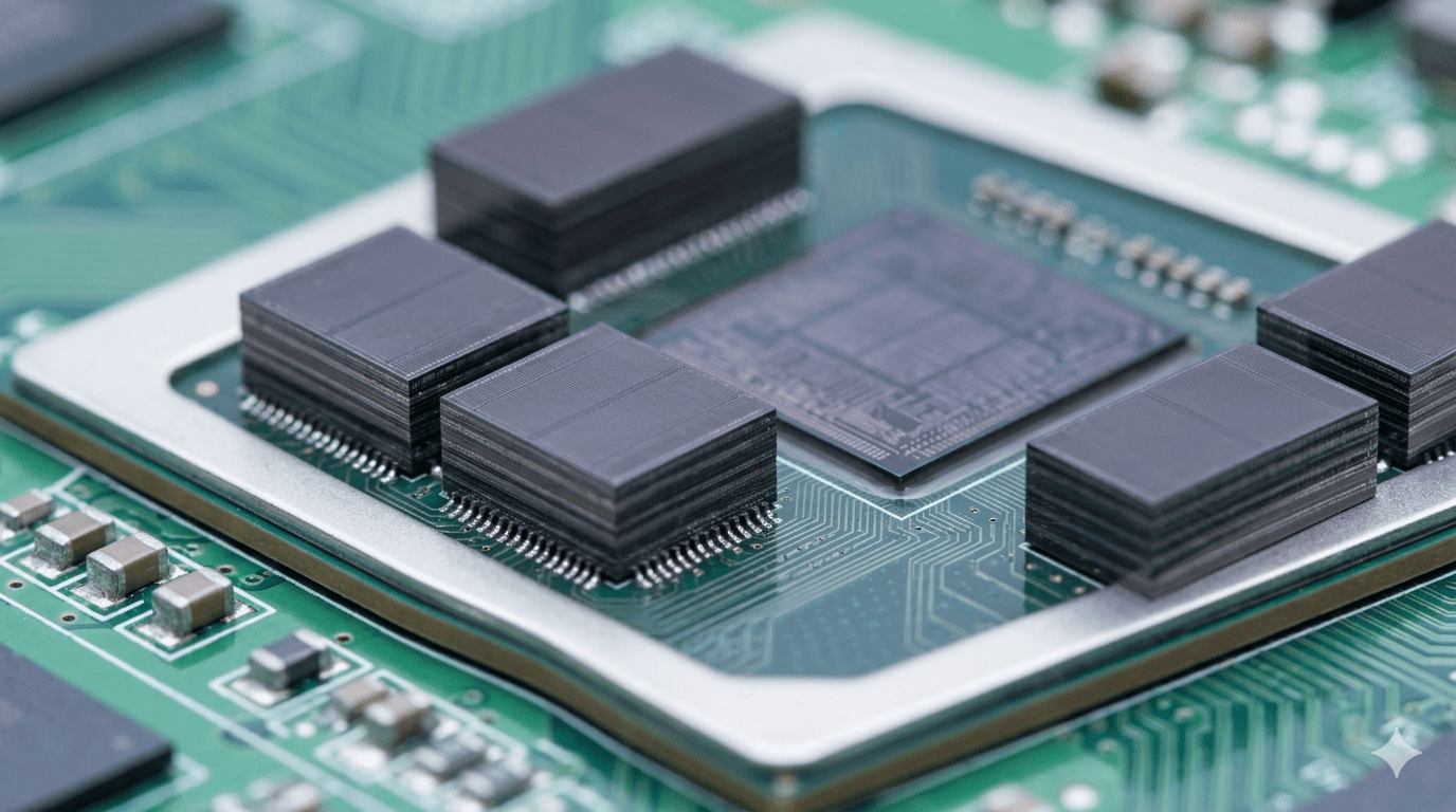
What High Bandwidth Memory Actually Does
Memory has become the new battleground in GPU evolution, and the reason is fundamental to how AI models work. Large language models and other AI systems do not just need raw compute. They need to move vast amounts of data between compute units and memory at extremely high speed. The bottleneck in AI inference is frequently not the arithmetic capability of the GPU. It is the speed at which the model’s weights can be loaded from memory into the compute units fast enough to keep them busy.
Standard DRAM, which connects to the processor over a conventional memory bus, cannot deliver data fast enough to saturate the compute capacity of modern AI accelerators. HBM solves this by stacking multiple DRAM dies vertically and connecting them to the processor through thousands of tiny connections called through-silicon vias. The result is memory bandwidth that is ten to fifteen times higher than conventional DRAM, delivered in a form factor that sits directly alongside the processor in the same package. That bandwidth is what allows modern AI accelerators to actually use their compute capacity rather than spending most of their time waiting for data.
NVIDIA’s H100 GPU uses HBM3, delivering around 3.35 terabytes per second of memory bandwidth. The Blackwell B200 uses HBM3e, pushing that further. The Vera Rubin generation will use HBM4, with bandwidth increases that compound the memory advantage of each hardware generation. Without corresponding increases in HBM supply and performance, each new GPU generation would be delivering more compute capacity than the memory system could actually feed, producing diminishing returns on the compute investment.
Why Supply Is the Real Problem
HBM is extraordinarily difficult to manufacture. It requires stacking multiple DRAM dies with extremely precise alignment and connecting them through micro-scale vias that must be fabricated without defects. The packaging process that bonds HBM stacks to GPU logic through TSMC’s CoWoS platform adds another layer of complexity. Only three companies, SK Hynix, Samsung, and Micron, currently produce HBM at commercial scale, and each faces its own yield and capacity constraints.
SK Hynix has been the dominant HBM supplier for NVIDIA’s most recent GPU generations, capturing the majority of the HBM market for AI applications partly through early technology leadership and partly through deep partnership with TSMC on the packaging integration. Samsung has been catching up but has faced yield challenges on HBM3e that delayed its qualification for Blackwell at scale. Micron entered the HBM market later and is ramping capacity, but the combined output of all three suppliers is still insufficient to meet the demand that the AI infrastructure buildout is generating.
The supply constraint manifests in two ways. First, HBM scarcity limits how many finished AI accelerators can ship, creating the capacity shortages that hyperscalers have been flagging in their earnings calls. Second, HBM costs represent a significant fraction of the total bill of materials for an AI accelerator, with HBM components for a single Blackwell NVL72 rack estimated at close to $50,000. That cost component feeds directly into the per-unit economics of AI compute and therefore into the pricing of cloud AI services.
What This Means for Infrastructure Planning
For enterprise and infrastructure operators, the HBM constraint creates planning implications that go beyond simply accepting that AI hardware is expensive and hard to get. The constraint is structural enough that it will shape hardware availability, pricing, and the economics of AI deployment for the next two to three hardware generations.
Operators planning significant AI infrastructure investments need to understand that the delivery timelines for AI accelerator orders are driven as much by HBM production ramp schedules as by GPU fab capacity. An order for Vera Rubin systems placed today is subject to when HBM4 production can supply enough stacks to build the ordered quantity. TSMC’s CoWoS packaging capacity is a second constraint in the same supply chain. Both of these constraints operate on timelines that are measured in quarters, not weeks, and that are not responsive to price signals in the way that commodity supply chains are.
The HBM supply chain is also a geopolitical variable in ways that conventional DRAM is not. The concentration of HBM production in South Korea, combined with the packaging concentration at TSMC in Taiwan, creates a supply chain geography that is sensitive to the same geopolitical pressures affecting other critical semiconductor supply chains. Operators building multi-year infrastructure strategies need to account for HBM supply security as a risk variable alongside GPU allocation and power availability.
The Architectural Response Taking Shape
The industry is not standing still in the face of HBM constraints. Several architectural responses are emerging that will change the memory landscape over the next hardware cycle.
Beyond GPUs, the hidden architecture powering the AI revolution includes memory innovations that go further than simply adding more HBM. Compute-in-memory approaches, which perform calculations directly within the memory array rather than moving data to a separate compute unit, could reduce memory bandwidth requirements for certain AI workloads by orders of magnitude. These approaches are still largely in research and early commercial stages, but several startups and established semiconductor companies are investing in them as a longer-term architectural alternative.
Near-memory compute, which places processing elements physically close to but not inside the memory, is a middle-ground approach that several companies are pursuing for AI inference applications. The goal is to reduce the data movement distance and therefore the energy and latency of the memory access, without requiring the full redesign of memory architecture that compute-in-memory demands.
The HBM supply constraint, like other infrastructure constraints in the AI buildout, will eventually ease as capacity investments come online and as architectural innovations reduce memory bandwidth requirements per unit of AI compute. Getting there will take several years and multiple hardware generations. The operators and enterprises who understand the constraint and plan around it, rather than assuming that hardware availability will match their demand on their preferred timeline, are the ones who will navigate this phase of the AI buildout most effectively.


