In today’s data centers, traditional electrical interconnects built on copper wiring are reaching hard physical limits. As AI accelerators and high‑performance compute systems scale to thousands of GPUs, moving ever‑larger volumes of data between chips and racks has become a major bottleneck. Silicon photonics, a technology that uses light instead of electricity to transmit information, has emerged as a practical solution. Consequently, it is rapidly gaining traction among data center architects and hyperscale operators.
Silicon photonics is not a speculative idea. Industry leaders such as Nvidia, TSMC, and Broadcom are developing products and roadmaps that place optical interconnects at the core of next‑generation networking hardware for AI and cloud workloads. This shift is more than a performance upgrade; it fundamentally changes how data flows inside and between the compute nodes powering modern digital services.
The Data Movement Problem in Modern Data Centers
For decades, electrical interconnects supported growth in processing power and bandwidth by scaling speeds on copper. As serial data rates increased from tens of gigabits to hundreds, copper wiring and pluggable optical modules kept pace. However, by 2026, these approaches are no longer sufficient for the demands of generative AI and hyperscale workloads.
Industry experts refer to this challenge as the “Copper Wall.” When data rates exceed 200 Gbps per lane, copper connections can often reach less than a meter before signal attenuation and crosstalk make them unreliable. Beyond this distance, maintaining signal integrity requires much higher power for amplifiers and signal conditioning. In large AI clusters, this has caused interconnects to consume a disproportionate share of total data center power.
Additionally, processor packaging introduces “shoreline bottlenecks,” where the edges of the chip can only accommodate a limited number of electrical I/O pins. As a result, raw compute performance can surpass the system’s ability to move data efficiently. This mismatch throttles performance, even if the silicon itself is capable of more.
What Silicon Photonics Is and Why It Matters
Silicon photonics integrates optical components such as lasers, modulators, detectors, and waveguides directly onto a silicon substrate. These components can be manufactured using existing CMOS fabrication processes. Instead of pushing electrical signals along copper traces, silicon photonics converts signals to light and transmits them over fiber or on‑chip optical paths. Photons generate far less resistance and heat than electrons, enabling higher bandwidth with lower energy loss.
This technology matters to data centers for three main reasons:
Higher Bandwidth: Optical links can handle data rates far beyond what copper can sustain. Current silicon photonics devices already achieve multi‑terabit per second throughput, with roadmaps targeting even higher speeds.
Lower Latency: By eliminating multiple electrical‑to‑optical conversions and creating direct paths between processors and networking fabrics, latency is reduced. For tightly coupled workloads, such as distributed AI training, this improvement translates into measurable performance gains.
Energy Efficiency: Optical transmission consumes less energy per bit and produces less heat than electrical signaling. This reduces stress on cooling and power infrastructure, which is particularly important for hyperscale operators in regions with grid limitations or high electricity costs.
Together, these benefits make silicon photonics a cornerstone technology for future data center interconnect design.
Co‑Packaged Optics: Bringing Light Close to the Silicon
One of the most transformative advancements in silicon photonics is co‑packaged optics (CPO). Traditional optical networking relies on separate transceiver modules at the edges of circuit boards. These modules convert electrical signals to optical signals and back again, adding power consumption, latency, and complexity.
CPO embeds optical engines directly alongside or within the same package as the switch ASIC or processor. Reducing the distance electrical signals must travel before conversion to light lowers both power consumption and latency while improving signal integrity. Industry data indicates that CPO can reduce interconnect power by roughly 3.5 times compared with traditional pluggable optics while also simplifying design and deployment.
Nvidia’s next‑generation switch platforms, including Spectrum‑X for Ethernet and Quantum‑X for InfiniBand, demonstrate silicon photonics and CPO in practice. These systems aim to deliver data rates of 800 Gbps and higher per port, enabling fabrics that can scale across thousands of GPUs without hitting I/O limits.
Scaling AI Workloads and “Non‑Blocking” Fabrics
AI workloads highlight why interconnect improvements are essential. Training a large language model or running distributed inference binds many processors together in synchronous operations. Any delays or bottlenecks in data movement slow down the entire compute job.
Silicon photonics enables what engineers call “non‑blocking fabrics,” where every node can communicate with every other node without bandwidth constraints. Optical interconnects provide the capacity and low latency necessary to build these fabrics at scale, from board‑level and rack‑level connections to inter‑rack and inter‑data‑center fabrics. This capability supports the next generation of AI factories, designed for massive models and real‑time inference across distributed resources.
Beyond hyperscale AI, optical interconnects also benefit high‑performance computing and cloud providers that must orchestrate compute resources efficiently to meet strict service level agreements and minimize latency for end users.
Industry Momentum and the Next Frontier
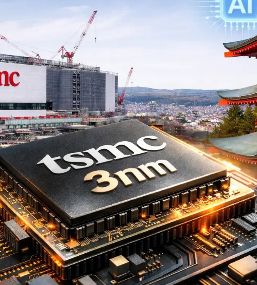
The adoption of silicon photonics is accelerating across the industry. TSMC’s Compact Universal Photonic Engine (COUPE) roadmap outlines integration stages from pluggable optical modules to full co‑packaged solutions capable of terabit‑scale speeds. This framework sets the stage for manufacturing silicon photonics at scale using advanced packaging techniques.
Meanwhile, Broadcom’s CPO‑based Tomahawk 6 switch and innovations from startups in photonic interposers show that optical I/O is moving from research labs into commercial products. These developments are attracting venture investment and strategic acquisitions, reflecting growing confidence in silicon photonics as a long‑term platform for data centers.
Real Challenges Remain
Scaling silicon photonics is not without obstacles. Manufacturing optical components that meet yield and reliability targets while remaining cost-effective is challenging. Precise fabrication and alignment of optical structures on silicon demand advanced process controls. Integrating optical and electrical components in co‑packaged systems adds design complexity and pushes existing packaging processes to their limits.
Standards and interoperability across vendors are still evolving. Since optical I/O represents a departure from decades of electrical networking norms, ecosystem coordination is necessary to ensure that different silicon photonics implementations work together seamlessly.
Despite these hurdles, the pace of development indicates that silicon photonics will become a core technology in next‑generation data center networks.
Light as the Backbone of Future Compute Fabrics
Silicon photonics addresses a fundamental truth of modern computing: raw processing power is meaningless if data cannot move efficiently between cores, chips, and racks. By shifting to optical data movement and embedding photonic components closer to compute silicon, data centers can overcome the I/O bottleneck that has slowed performance scaling for years.
For hyperscale operators and cloud infrastructure planners, adopting silicon photonics delivers higher throughput, lower latency, and better energy efficiency. These improvements will be essential as AI models continue to grow in size and complexity and as the demand for faster, greener data centers increases.
Moving data at the speed of light may sound like a cliché, but with silicon photonics, it is becoming a practical reality that redefines the limits of compute infrastructure.


