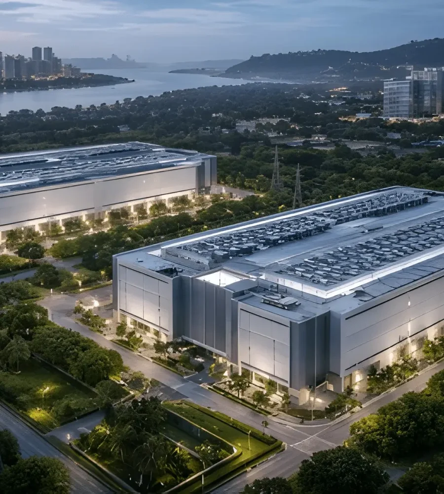
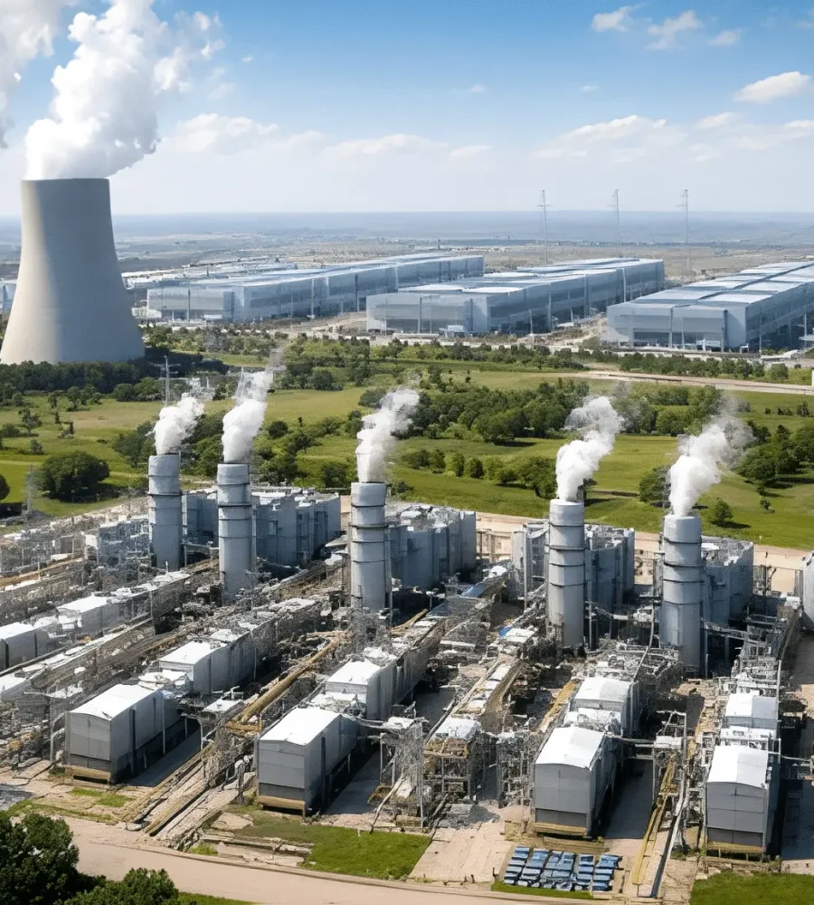
Technologists are moving away from the era of general-purpose central processing units. Instead, they are embracing a new paradigm of accelerated computing. This transition is not merely a hardware upgrade. Rather, it represents a wholesale restructuring of modern infrastructure. This shift is driven entirely by the unique requirements of large-scale artificial intelligence. Traditional semiconductor scaling paradigms have reached their physical and economic limits. Consequently, the emergence of AI-optimized silicon is forcing a total reimagining of data centers and energy networks. This silicon features massive parallelization and heterogeneous integration. Furthermore, the shift from Moore’s Law to Huang’s Law signifies the birth of the AI Factory. In this new model, the primary output is no longer data storage. Instead, these facilities focus on the systematic generation of intelligence as a utility.
The Death of the General-Purpose Era
For decades, the semiconductor industry followed the predictable cadence of Moore’s Law. This principle posited that the number of transistors on a dense integrated circuit would double approximately every two years. This scaling provided a reliable roadmap for increasing computational density. However, transistor geometries have now approached the single-digit nanometer scale. As a result, the industry has encountered insurmountable physical challenges. These include quantum tunneling and thermal leakage. Technologists now observe that Moore’s Law has slowed significantly. Therefore, traditional chips can no longer meet the performance demands of modern probabilistic workloads.
The Ascendancy of Huang’s Law
Huang’s Law has emerged as the new governing principle in this vacuum. Jensen Huang, the CEO of NVIDIA, lends his name to this observation. This law posits that graphics processing unit performance is growing at a much faster rate than central processing units. Specifically, AI performance now doubles every six months to a year. This hyper-accelerated pace is fueled by a synergy across the entire computing stack. This includes architecture, interconnects, and memory technology. Moreover, software efficiency plays a critical role. While Moore’s Law focused on hardware alone, Huang’s Law claims that full-stack orchestration makes this progress possible.
The Efficiency Gap in Infrastructure
Modern infrastructure is no longer a simple container for servers. Instead, it is becoming a single, integrated AI Factory. In this model, the silicon dictates the power and cooling. The infrastructure must follow the requirements of the chip. Consequently, the boundaries between hardware and physical buildings are disappearing. CPUs are designed for sequential tasking. However, they are fundamentally inefficient for the massive matrix multiplications that AI requires. This efficiency gap has created a bottleneck in the AI-first economy. Therefore, companies are shifting toward specialized accelerators.
Economic Logic and Asset Depreciation
This shift has profound implications for infrastructure ownership. In the Moore’s Law era, hardware followed a five-to-seven-year depreciation cycle. However, AI hardware delivers massive performance improvements within just two years. This rapid innovation renders existing infrastructure economically obsolete very quickly. For instance, new AI chips can be eight times faster than models from just two years ago. Therefore, organizations must transition from capital expenditure models. They are now prioritizing flexibility and operational access to the latest silicon generations.
The Silicon Architecture: The Chiplet Revolution
The industry has reached the physical size threshold for printing single chips. This is known as the reticle limit. Consequently, monolithic processor designs have become impractical for high-performance AI tasks. Manufacturers have responded with a modular approach. This is the Chiplet Revolution. In this paradigm, designers stitch together smaller, specialized silicon components. They use advanced 2.5D and 3D packaging technologies to accomplish this. This transition represents a modularization of silicon. As a result, manufacturers can combine diverse process nodes into a single system-on-package.
Heterogeneous Integration Strategies
Major semiconductor players fully embraced this heterogeneous integration by early 2026. For example, Intel utilized its 18A node and Foveros Direct 3D packaging. This technology allows for a 9-micrometer copper-to-copper bump pitch. This represents a tenfold increase in interconnect density. Intel uses these techniques for its Clearwater Forest Xeon processors. Furthermore, Intel moved toward PowerVia technology. This involves backside power delivery to improve energy efficiency. These complex stacks ensure higher performance for AI workloads.
AMD and the CDNA Architecture
Similarly, AMD leverages TSMC’s CoWoS packaging for its Instinct MI400 series. This architecture integrates high-performance logic with massive HBM4 memory. It achieves a staggering bandwidth of 19.6 TB per second. The modularity provides a clear economic advantage. Manufacturers achieve higher yields by using smaller dies. A single defect no longer ruins an entire massive chip. Instead, it only affects one replaceable chiplet. Consequently, this modular approach results in a 33 percent lower total cost of ownership.
The Universal Chiplet Ecosystem
The maturation of the Universal Chiplet Interconnect Express (UCIe) 3.0 standard is pivotal. This open standard creates a multi-vendor ecosystem. It allows components from different manufacturers to communicate seamlessly. For instance, an enterprise can combine an Intel compute tile with an NVIDIA accelerator. They can also add Samsung memory into the same physical package. This interoperability breaks the proprietary hold of individual chipmakers. Moreover, it accelerates innovation cycles across the entire industry.
Memory Architectures: High-Bandwidth Memory 4
AI-optimized silicon is only as effective as its memory subsystem. Large language model inference is frequently memory-bound. This means the speed of the processor is limited by data retrieval. This phenomenon is often called the Memory Wall. Therefore, the emergence of High-Bandwidth Memory 4 (HBM4) is a critical milestone. This technology is essential for overcoming data bottlenecks in 2026. It allows AI models to process trillion-parameter data sets efficiently.
Technical Breakthroughs in HBM4
HBM4 departs from previous standards in several ways. It doubles the interface width from 1024 bits to 2048 bits. This wider pipe allows for massive data throughput without extreme clock speeds. Consequently, the thermal profile remains manageable. A single 16-layer stack can now exceed 2 TB per second in bandwidth. Furthermore, SK Hynix utilized Advanced MR-MUF technology to achieve this density. They thinned DRAM wafers to approximately 30 micrometers. This is about one-third the thickness of a human hair.
The Logic Die and Co-Processing
The innovation of HBM4 extends to the base of the memory stack. In a strategic shift, memory makers are manufacturing logic dies on advanced 5nm nodes. This transforms the HBM into an active co-processor. The logic die can pre-process data before it reaches the GPU. This reduces the load on the main accelerator. When integrated into platforms like NVIDIA Vera Rubin, a single GPU can access 384GB of high-speed memory. This creates an aggregate bandwidth of over 22 TB per second.
Strategic Alliances in Memory
The memory market has moved away from traditional commodity cycles. HBM4 is now a custom-designed infrastructure component. Consequently, major hyperscalers have already pre-sold most of the 2026 production capacity. Companies like Meta and Google signed multi-year supply contracts to secure their needs. This prioritization has created a secondary effect on the broader market. Standard DDR5 supply is beginning to dry up. Therefore, analysts expect price increases of 15 to 20 percent for consumer electronics by mid-2026.
The Power Paradox: From 48V to 800V
Silicon innovation is forcing a total overhaul of electrical engineering. Traditional 48V power distribution architectures are struggling. They cannot support the high power density of modern AI racks. Modern AI clusters now require megawatts of power. Consequently, NVIDIA and its partners are leading a transition to 800V High-Voltage Direct Current (HVDC) infrastructure. This shift reduces energy loss and minimizes the need for heavy copper cabling.
Efficiency of HVDC Systems
Traditional data centers use multiple conversion steps. These steps introduce significant energy losses. However, the 800V HVDC model converts grid power directly at the data center perimeter. This eliminates intermediate conversion steps. As a result, end-to-end efficiency improves by up to 5 percent. Maintenance costs also drop by up to 70 percent. Furthermore, the 800V architecture allows wires to carry 157 percent more power. This enables a 45 percent reduction in copper usage across the facility.
Single-Stage Conversion Innovations
Within the compute node, innovators use high-ratio converters. These step the voltage down to 12V DC immediately adjacent to the GPU. This single-stage conversion is highly efficient. It occupies 26 percent less area than traditional approaches. This frees up valuable real estate near the processor. This foundation is essential for supporting future racks. For instance, the NVIDIA Kyber architecture will support IT loads exceeding 1 MW per rack.
The Energy Frontier: Small Modular Reactors
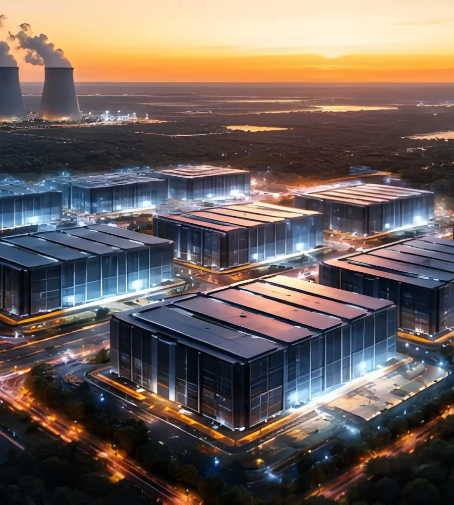
The energy appetite of AI is insatiable. Consumption is projected to double by 2028. This strain on the electric grid is turning power into a bottleneck. Consequently, hyperscalers are exploring Small Modular Reactors (SMRs). These reactors provide a dedicated and carbon-free power source. SMRs offer a stable baseload supply that is less vulnerable than solar or wind. Moreover, their modular design allows for faster deployment.
Hyperscaler Investment in Nuclear
Major technology companies are making massive investments in nuclear power. For example, Meta announced a procurement of 6.6 GW of nuclear energy. They are partnering with firms like TerraPower and Oklo. Similarly, Google and Amazon are backing SMR development. These reactors are factory-manufactured. Then, they are transported to operational sites. This modular approach allows operators to add capacity incrementally as compute demand grows.
Civil Engineering for SMR Campuses
Integrating SMRs into AI campuses introduces a rigorous engineering framework. Civil engineers must plan for security setbacks and controlled-access zones. They must also design protected underground corridors for power and cooling water. Furthermore, the heat rejection system must be highly redundant. Depending on the reactor type, this could be a closed-loop tower or a dry-cooling array. Engineers must ensure these systems operate independently to guarantee safety and uptime.
Utility and Interconnection Strategies
The electrical architecture of an SMR-enabled campus is complex. It must balance behind-the-meter generation with grid resilience. Civil teams should design for dual-feed arrangements. This includes a short tie to the data center switchyard. It also includes a regulated grid intertie for power export. Moreover, isolation must be maintained at points of coupling. Utility protection schemes must harmonize with the nuclear plant’s safety systems. This ensures a stable and reliable power ecosystem.
Thermal Infrastructure: Liquid is the New Air
AI silicon is optimized for 100kW or more per rack. Consequently, air cooling is physically impossible. AI silicon is literally killing the traditional data center layout. This includes the end of the traditional raised floor. Modern AI hardware is much denser and heavier than legacy equipment. A standard server rack weighs around 1,000kg. However, modern AI racks can weigh up to two tonnes.
The Physics of Heavy Infrastructure
This weight differential creates a major problem for existing buildings. Legacy data centers were engineered for standard server density. Therefore, the cumulative weight of AI racks often exceeds structural load limits. Reinforcing existing floors is very expensive. It often costs as much as new construction. As a result, the industry is shifting toward concrete slab floors. Furthermore, sprawling single-story layouts are becoming more popular. These designs manage the immense weight more easily.
Direct-to-Chip and Immersion Cooling
Liquid cooling has become the industry standard for 2026. Operators use advanced methodologies to manage thermal loads. Direct-to-chip cold plates involve mounting liquid-cooled blocks on GPUs. Moreover, immersion cooling submerges entire server chassis in dielectric fluid. This allows for extreme hardware density. Some liquid-cooled centers achieve power usage effectiveness scores below 1.1. This represents a significant improvement in energy efficiency.
Rear Door Heat Exchangers (RDHx)
Rear Door Heat Exchangers serve as a vital bridge technology. They allow operators to retrofit legacy air-cooled facilities. RDHx systems neutralize hot exhaust air at the source. They return it to the room at near-ambient temperature. Furthermore, active RDHx systems can handle thermal loads exceeding 200 kW per rack. These systems use independent fans with variable speed control. Consequently, they enable high-density AI racks to coexist with lower-power hardware.
The Sovereign Silicon Shift
Infrastructure is now a matter of national security. The strategic importance of AI has led to the rise of Sovereign AI. This refers to the ability of nations to govern their own AI ecosystems. If a nation relies on third-party clouds, its intelligence is effectively leased. Therefore, countries are racing to build their own national compute reserves. These initiatives involve billions of dollars in public and private investment.
Custom Cloud Silicon Development
Hyperscalers like AWS, Google, and Microsoft are building their own chips. They want to bypass the high margins of third-party vendors. For example, AWS developed the Trainium 3 chip on a 3nm process. Google introduced the TPU v7 Ironwood for high-volume inference. Microsoft launched the Maia 200 accelerator to power its GPT-5.2 models. Notably, custom silicon can be 50 to 70 percent cheaper than high-end GPU clusters. This allows cloud providers to control their own performance and cost destiny.
The IndiaAI Mission
India has taken a leadership role in sovereign infrastructure. The government approved the IndiaAI Mission with a massive budget. This mission aims to build a national compute reserve of over 18,000 GPUs. They are using a public-private partnership model to achieve this. This initiative treats AI infrastructure as essential national digital infrastructure. Consequently, startups and researchers can access affordable compute at 40 percent reduced costs. Moreover, India will host the first-ever global AI summit in the Global South in 2026.
EU AI Factories and Gigafactories
The European Union is pursuing its own technology sovereignty. The EU Action Plan includes a 200 billion euro investment. This initiative aims to triple the EU’s compute capacity by 2027. Specifically, it involves the creation of thirteen AI Factories across member states. Furthermore, the EU is building AI Gigafactories. These are large-scale facilities capable of training frontier models. They will host over 100,000 advanced processors per installation. This ensures Europe remains competitive in the global AI race.
Networking: The Fabric is the Computer
In an AI-optimized world, the network is the computer. AI clusters grow to encompass tens of thousands of GPUs. Consequently, the networking fabric has become as critical as the silicon itself. Modern AI workloads require both scale-up and scale-out networking. Scale-up happens within a rack or pod. Conversely, scale-out connects resources across the entire data center. Both levels are necessary to maintain the feel of a single unified compute space.
NVLink and the Scale-Up Interconnect
NVIDIA’s NVLink remains the gold standard for scale-up networking. The fifth-generation NVLink enables a bandwidth of 130 TB per second. This allows an entire rack of 72 GPUs to operate as a single massive processor. For multi-vendor environments, the Ultra Accelerator Link (UALink) has emerged. This protocol allows multiple compute nodes to share a unified address space. Furthermore, it aims to scale to over 1,000 accelerators per workload.
The Battle Between InfiniBand and Ethernet
A fierce competition is underway for scale-out networking. InfiniBand is currently the performance leader for large-scale training. It offers ultra-low latency and deterministic performance. However, the Ultra Ethernet Consortium (UEC) has launched a powerful counterattack. The UEC 1.0 specification reconstructs the network stack for AI performance. Moreover, Ethernet’s ubiquitous ecosystem and lower cost make it attractive for enterprise AI. Consequently, Ethernet is expected to gradually expand its market share.
Silicon Photonics and Optical Interconnects
Copper interconnects are reaching their physical limits. They struggle to maintain signal integrity beyond one meter at high speeds. Therefore, the industry is shifting toward optical I/O. Silicon photonics involves moving optical engines directly onto the chip package. For instance, Ayar Labs’ TeraPHY chiplet delivers 8 TB per second of bandwidth. This eliminates distance barriers while reducing power consumption. Furthermore, NVIDIA announced co-packaged optics switches for 2026. These innovations provide higher network resiliency and better efficiency.
The Workforce and FinOps Shift
The restructuring of infrastructure touches on human and economic impacts. The transition from the training era to the inference era is critical. Efficiency per token now determines the profitability of a company. Organizations are moving away from tracking total monthly spend. Instead, they focus on cost per successful interaction. This granularity exposes which features are draining margins. Therefore, FinOps for AI has become a mandatory discipline for enterprises.
Inference Economics and Model Right-Sizing
Inference costs have plummeted at an unprecedented rate. They dropped 280-fold over the last two years. For example, GPT-4 equivalent performance cost just 40 cents per million tokens in late 2025. This commoditization of intelligence is driving new strategies. Organizations now practice aggressive model right-sizing. They use the smallest model possible to meet a quality bar. For instance, a routine task might route to a micro-model costing very little. This preserves margins without affecting user experience.
Quantization and Speculative Decoding
Technologists use specific techniques to reduce inference costs. Quantization lowers the numerical precision of model parameters. This saves memory and speeds up computation. Consequently, models can run on more cost-effective hardware. Moreover, speculative decoding enhances throughput. This method uses a small draft model to generate tokens quickly. Then, a larger model verifies them in a single pass. Together, these techniques yield significant efficiency gains for production AI.
The Specialized Labor Gap
The transformation of data centers is creating a massive talent gap. IT teams must transition from traditional server management to specialized operations. These include GPU cluster management and advanced thermal systems. Consequently, new roles like Senior AI Factory Cooling Engineer are emerging. These professionals must understand both AI model weights and industrial fluid dynamics. Moreover, they need proficiency in digital twins and computational fluid dynamics. This hybrid knowledge is rare but essential for modern AI factories.
Reskilling and Infrastructure Operations
Network architects also face major challenges. They must design for AI-first traffic patterns. These differ fundamentally from traditional enterprise networking. For instance, GPU-to-GPU communication requires ultra-low latency and massive throughput. Many organizations lack the expertise to design these fabrics. Therefore, businesses are investing heavily in workforce development. They are training staff in hybrid compute portfolio optimization. This includes mastering financial models that account for GPU utilization and inference economics.
Implementation of AI Governance Frameworks
In 2026, AI regulation continues to evolve globally. Countries are transitioning from drafting to implementing regulatory frameworks. For example, EU member states are focusing on the AI Act. Meanwhile, nations in the Asia-Pacific region are adopting innovation-preserving frameworks. Japan and Canada are modernizing privacy laws to account for AI risks. Furthermore, India is implementing newly passed legislation for data protection. These rules will define how AI factories operate in the coming years.
The Role of FinOps in AI Governance
Technology leaders are integrating FinOps directly into AI governance. They create cross-functional teams that include finance and data science. These teams work together to balance performance and value. They use predictive analytics to forecast budget impacts before workloads scale. Moreover, they experiment with new pricing models like universal tokens. This aligns costs with actual business value delivery. Consequently, engineers now see financial efficiency as a measure of innovation.
Managing AI Infrastructure Risk
Enterprises face a reckoning regarding AI infrastructure costs. Many organizations underestimate these expenses by up to 30 percent. The reason is often under-forecasting the operational overhead of inference. Inference workloads run continuously, consuming cycles long after training ends. Therefore, companies need real-time observability across the AI lifecycle. They must track how much each model costs to serve. This clarity allows for better strategic navigation through market turbulence.
The Industrialization of Intelligence
The restructuring of infrastructure around AI silicon represents a permanent shift. The transition from Moore’s Law to Huang’s Law has invalidated old strategies. Instead, the world is moving toward modular chiplet designs and 800V HVDC power. High-bandwidth memory and silicon photonics are now essential components. Furthermore, nations are building sovereign compute reserves to protect their strategic interests. Hyperscalers are even turning to nuclear power to meet energy demands. Intelligence is effectively becoming a commoditized utility. This industrial revolution of compute is creating a new economic foundation. Organizations that master this infrastructure metamorphosis will command the most leverage. They will define the future of the 21st-century digital economy.


