
The Energy Abundance Fallacy
Elon Musk said it at the World Economic Forum in Davos in January 2026, and the comment spread through the AI infrastructure conversation like a policy directive: the limiting factor for AI deployment is fundamentally electrical power, and China’s growth in electricity is tremendous. The implication, widely absorbed, was that energy abundance translates directly into AI infrastructure dominance. China builds more renewable capacity than any other nation. China’s grid is expanding faster than any comparable economy. Therefore China wins the AI power race.
That logic is clean and almost entirely wrong. Electricity and operational AI infrastructure are not the same thing, and the gap between them is precisely where East Asia’s most consequential infrastructure story is unfolding in 2026. China does have abundant, cheap electricity. It also has data centres that sit idle, a national computing initiative that has fuelled speculative overbuilding and inter-provincial competition rather than coordinated capability, a domestic chip mandate that writes out the world’s most capable AI hardware from its largest procurement programme, and a memory technology gap that costs its AI companies measurable months of model development time. South Korea, meanwhile, controls the memory technology that underpins every frontier AI chip globally, is scaling production at a pace that has made HBM a strategic national asset, and is simultaneously confronting a thermal crisis at the chip stack level that threatens to constrain the very hardware advantage it is racing to extend.
Neither narrative fits the clean triumphalism or clean alarm that AI coverage tends to prefer. What emerges from examining both countries’ actual infrastructure conditions, rather than their headline energy statistics, is a more complex and more instructive picture: East Asia is not a monolithic AI infrastructure power. It is a region of genuine, specific, consequential advantages intersecting with genuine, specific, consequential constraints, and understanding which is which matters considerably more for assessing the AI competition than any summary statistic about gigawatts or gigafactories can convey.
China’s East Data, West Computing: The Initiative That Overshot Its Own Logic
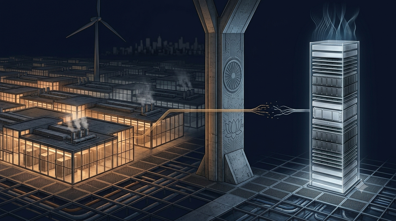
China’s Eastern Data, Western Computing initiative, launched formally in February 2022 following a period of pilot development across eight national hub regions, represents one of the most ambitious pieces of national computing infrastructure policy any government has ever attempted. The strategic logic is elegant in its simplicity. China’s most compute-intensive users and enterprises are concentrated along the eastern seaboard, in Guangdong, Jiangsu, Shanghai, and Beijing. China’s most abundant and cheapest renewable energy is in the west and northwest, in Guizhou, Inner Mongolia, Gansu, and the Ningxia Hui Autonomous Region, where land is inexpensive, temperatures are cooler, and wind and solar resources are abundant by any global standard. Moving data processing from where demand is to where power is cheap and green simultaneously reduces operational costs and advances carbon commitments.
Connecting those geographies through a national computing network, routing workloads that tolerate latency, primarily training and batch processing, from eastern demand centres to western infrastructure hubs via high-bandwidth fibre links, is a coherent response to the specific geographic mismatch that China’s energy and demographic distribution creates. A data centre in Inner Mongolia running on cheap wind electricity and processing training jobs submitted from a Beijing AI lab is, in principle, a more economical and more sustainable arrangement than building another data centre in Beijing and running it on the eastern grid’s more expensive and more carbon-intensive power mix.
The project has also contributed to genuinely significant carbon outcomes when modelled across scenarios. A ScienceDirect analysis of the initiative’s energy and emissions trajectory projected cumulative CO2 equivalent reductions measured in hundreds of millions of tonnes through 2030 under optimistic deployment scenarios, with the potential to meet China’s interim net-zero objective for the data centre industry ahead of schedule if PUE optimisation is pursued in parallel with the geographic redistribution. Electricity costs in data centres account for approximately seventy percent of operational expenses in the Chinese market, and the electricity price differential between western hub regions and major eastern cities represents an operational cost advantage that compounds significantly at the scale of a national computing network. The architecture of the initiative is right. The execution has encountered structural obstacles that the architecture did not anticipate.
The Utilisation Problem That Energy Abundance Cannot Solve
The ASPI Strategist’s May 2026 analysis of the EDWC initiative’s operational reality is the clearest-eyed assessment of the gap between the initiative’s geographic logic and its actual performance, and it opens with a direct challenge to the Musk-style energy abundance argument: China’s data-centre expansion under EDWC reveals that abundant, cheap power alone is no reliable sign of a unified, operable computing network. The consequence of the initiative in practice has not been a coherent national computing grid. It has been a collection of partially-utilised facilities built in locations that made sense for energy costs but that face operational constraints none of the energy analysis anticipated.
The specific form that EDWC’s overbuilding has taken reflects a structural incentive problem embedded in how provincial governments compete for central government recognition and investment. Each provincial administration has an institutional incentive to demonstrate that it is actively participating in national AI infrastructure development, which translates into data centre construction commitments that are calibrated to the appearance of strategic engagement rather than to validated demand signals. The result, documented by the ASPI analysis, is inter-governmental competition and speculative semiconductor stockpiling that has diverted resources from priority sectors while leaving many data centres idle. China began introducing electricity subsidies of up to fifty percent for data centres using domestically-produced semiconductors in November 2025, specifically because weak demand was failing to meet the expectations that the EDWC construction programme had been built around. Subsidising energy costs to incentivise utilisation of infrastructure that was built speculatively is not a sign of a programme working as designed.
The latency constraint that the east-to-west routing architecture imposes on certain workload categories adds a physical dimension to the utilisation problem that subsidies cannot address. Enterprise inference workloads, the continuously-running, latency-sensitive AI applications that represent the fastest-growing share of total AI compute demand globally, require round-trip times between user and data centre that are incompatible with the east-to-west transit latency of even China’s most advanced fibre infrastructure. An AI customer service application serving Shanghai enterprises from a data centre in Guizhou is not an architecture that any latency-sensitive commercial deployment can accept, which means that the western hub facilities are structurally limited to the batch processing and training workloads for which they were originally designed, while inference demand continues to concentrate in the eastern markets where grid costs are higher and the renewable energy story is less compelling. EDWC moved the training infrastructure west. The inference demand has not followed it.
The Two Trillion Yuan Mandate and Its Hardware Contradiction
The announcement reported by Bloomberg on June 9, 2026 describes a programme of a scale that has no precedent in the history of national computing infrastructure investment. China’s National Development and Reform Commission has been developing a five-year, two-trillion-yuan plan, equivalent to approximately two hundred and ninety-five billion dollars, to connect thousands of data centres into a unified national computing grid, with a mandate that at least eighty percent of the underlying technology, including AI accelerator chips, come from domestic suppliers. On the day Bloomberg published its report, Nvidia shares fell two point four percent and AMD dropped four percent, a market reaction that reflected the programme’s explicit structural exclusion of the world’s two most capable AI chip designers from the largest single computing procurement in history.
The programme builds directly on the EDWC architecture, fitting within Beijing’s broader Six Networks infrastructure strategy and using the hub-and-spoke geographic distribution that EDWC established as its physical foundation. The scale of public commitment, combined with Goldman Sachs’s separate estimate that China’s top internet firms will spend over seventy billion dollars on data centre capital expenditure by 2027 independently of this state programme, establishes a capital commitment to Chinese AI infrastructure that is genuinely formidable in absolute terms. The eighty percent domestic content mandate simultaneously creates the largest guaranteed revenue pool in history for China’s domestic semiconductor industry, primarily Huawei’s Ascend chip ecosystem, and locks out the performance baseline that would otherwise anchor the new grid’s capability.
The NDRC mandate creates a direct commercial consequence for Huawei that is not ambiguous. Huawei shipped approximately eight hundred and twelve thousand Ascend chips in 2025 and projects roughly twelve billion dollars in AI processor revenue for 2026, a roughly sixty percent increase from the prior year. If the two-trillion-yuan programme mobilises procurement at the scale its headline figure implies, and if the eighty percent domestic content requirement holds, Huawei’s chip revenue trajectory could be transformed. The supply constraint that currently limits this trajectory is not political will but manufacturing capacity: SMIC, China’s most advanced domestic foundry, operates at process nodes that are several generations behind TSMC’s capability for advanced AI chips, and the gap between Ascend hardware performance and Nvidia’s current generation directly translates into longer model training times for AI companies forced to use it.
The Ecosystem Gap That the Mandate Exposes
Mandating domestic hardware at scale is a coherent industrial policy instrument. It generates the revenue that funds the next generation of development, creates the installed base that builds the developer ecosystem, and reduces the foreign dependency that export controls exploit. The instrument’s effectiveness, however, depends on the domestic alternative being capable enough to perform the required function at a standard that does not impose prohibitive capability penalties on the enterprises and institutions using it. The RAND Corporation’s documentation of iFlytek’s experience, in which the major Chinese AI company reported a three-month delay in model development time when it switched from Nvidia hardware to Huawei’s Ascend 910B chips for training, provides the most concrete measurement of what the hardware performance gap costs in operational terms.
Three months of additional model development time, in an AI competitive environment where the gap between releasing a model ahead of rivals and releasing it after them is commercially and strategically significant, is not an acceptable penalty for any company competing at the frontier. DeepSeek’s acknowledgment that peak throughput would remain constrained until Ascend 950PR supernodes ship in volume in the second half of 2026, combined with its researchers’ documented rewriting of their own algorithms specifically to work within Ascend’s architectural constraints, illustrates that the performance gap imposes costs not just in time but in engineering talent diverted from model development toward hardware accommodation. When the world’s most efficient open-weight AI model must invest meaningful research effort in making its code work on the hardware its government is mandating, the mandate’s net effect on the quality and pace of Chinese AI development is meaningfully negative, even if its effect on Huawei’s revenue and China’s domestic semiconductor development trajectory is positive.
Huawei’s late-2025 announcement that it would open-source both its CANN toolchain and its MindSpore framework by year-end 2026 was, as the Techtimes analysis noted, a direct acknowledgment that ecosystem maturity is its most significant competitive deficit. CUDA’s dominance over the developer ecosystem, accumulated through more than a decade of documentation, optimisation, and community development, cannot be overcome by opening a toolchain in a single announcement. The practical friction that Huawei’s own CANN platform creates when developers port CUDA-optimised production code to it, including performance regressions and debugging overhead that CUDA workflows do not generate, is an operational reality that the developer community encounters regardless of what the political and commercial mandate says about which hardware to use. China’s AI infrastructure buildout will run faster, at higher hardware utilisation, and with less developer friction, when Ascend closes the performance and ecosystem gap against Nvidia. That gap is narrowing. The speed at which it narrows determines the effective capability of the two-trillion-yuan grid.
South Korea and the Memory Choke Point
Two companies in one country control ninety percent of a component that every frontier AI system in the world depends on. Samsung Electronics and SK Hynix produce the overwhelming majority of global High Bandwidth Memory, the specialised DRAM stacked in multi-layer packages directly adjacent to AI accelerator chips that provides the memory bandwidth without which large-scale AI inference and training cannot function at commercially viable speeds. This is not a minor supply chain dependency. It is a structural chokepoint in the global AI hardware supply chain that is more concentrated, more technically complex, and more strategically consequential than the public discussion of AI chip competition has fully absorbed.
HBM differs from conventional DRAM in its architecture in ways that make it genuinely difficult to produce at competitive yield and performance. Multiple DRAM dies are stacked vertically and connected through thousands of microscopic through-silicon vias, then bonded to a logic die at the base using advanced packaging techniques that require wafer-level precision across the entire stack. This manufacturing complexity, combined with the enormous research investment required to advance each successive generation, has produced a market structure where meaningful volume production is achievable only by the companies that have been investing in this specific technology for the longest period at the highest capital intensity. SK Hynix held fifty-three percent of the HBM market in the third quarter of 2025. Samsung held thirty-five percent. Micron held eleven percent. Everything else in the global AI chip supply chain, from the Nvidia GPU to the hyperscaler inference cluster, depends on the production decisions of these three companies, with South Korean manufacturers controlling close to nine in ten units shipped.
HBM4 mass production began in February 2026, marking what Introl’s analysis described as the most significant architectural overhaul in memory technology history. The JEDEC JESD270-4 standard defines a doubling of interface width from 1024 bits to 2048 bits and an expansion of channels from 16 to 32, producing bandwidth capabilities that previous generations could not approach. Nvidia’s Vera Rubin architecture depends entirely on HBM4 availability. OpenAI’s Stargate project has received a nine-hundred-thousand-wafer-per-month commitment from South Korean producers. Server DRAM prices surged sixty to seventy percent in the period preceding HBM4 launch. The HBM market total addressable market is projected to reach one hundred billion dollars by 2028, up from thirty-five billion dollars in 2025. The supercycle framing that Bank of America applied to the memory market, predicting conditions similar to the semiconductor boom of the 1990s, reflects both the genuine demand trajectory and the concentrated supply structure that makes pricing power unprecedented in the industry’s history.
The Thermal Wall That the Next Generation Must Climb
The same power density increase that is reshaping data centre cooling infrastructure globally is arriving at the chip stack level in a form specific to HBM’s physical architecture, and the thermal management challenge this creates is the next competitive frontier for South Korean memory manufacturers. Power consumption of next-generation AI server GPUs from Nvidia and other vendors is trending toward one thousand watts per chip, a figure that was unthinkable at the time HBM’s foundational architecture was specified and that imposes thermal demands on the memory stack directly bonded to those chips that previous generations of HBM engineering were not designed to manage.
HBM is not simply attached to an AI accelerator die. It is physically stacked and bonded adjacent to it in a package-level integration that maximises bandwidth by minimising signal path length. The consequence is that the thermal output of the GPU flows directly into the memory stack through the same substrate that connects them electrically, with no air gap, no separate cooling path, and no thermal break between a chip drawing close to one thousand watts and the memory dies bonded to it. As GPU thermal design power has increased from generation to generation, the thermal environment that HBM must survive inside the package has grown correspondingly more challenging, creating a situation where memory reliability and performance are being constrained not by the memory die itself but by the heat generated by the logic chip it is paired with.
Samsung, SK Hynix, and Micron are all investing in dedicated thermal management innovations for the HBM5 generation and beyond, with TrendForce’s June 2026 analysis documenting that all three companies are placing greater emphasis on cooling and power-efficiency technologies as Nvidia and AMD push HBM suppliers to enhance thermal control and low-power design capabilities. SK Hynix has specifically introduced what it calls the iHBM solution, targeting a thirty percent thermal resistance reduction for HBM5 adoption. Micron’s 2025 US patent on stacked memory thermal dissipation describes a vertical heat-management structure using electrically passive cooling through-silicon vias that form a low-resistance vertical thermal path operating in parallel with the electrical TSV network, essentially building a dedicated heat highway into the memory stack itself. Samsung is pursuing thermally conductive interface layer innovations at the die-attach level. These are not incremental refinements of the cooling approach. They are fundamental architectural changes to how heat is managed inside the memory package, driven by the recognition that the GPU thermal wall is now a memory engineering problem as much as a chip design problem.
South Korea’s Domestic Infrastructure and the Fab Power Drain
The HBM supercycle has an infrastructure dimension that extends beyond the chip itself and into the domestic South Korean power grid. Samsung’s P5 facility in Pyeongtaek, Gyeonggi, currently under construction with expected operational status by 2028, and SK Hynix’s M15X facility in Cheongju, Chungcheongbuk-do, slated for utilisation by mid-2027, represent the production capacity expansion that the HBM demand trajectory requires. These are not modest additions to existing manufacturing capacity. They are among the largest semiconductor fabrication investments in South Korean history, requiring power infrastructure at a scale that places measurable demands on the regional grids serving Gyeonggi and Chungcheongbuk-do.
South Korea faces a version of the same infrastructure timing problem that Europe and the United States are navigating: semiconductor fabrication facilities require secure, high-quality power supply that must be available when the fab comes online, not years after it has already commissioned its production lines. Grid investment in South Korea has not kept pace with the semiconductor capital expenditure commitments that the HBM supercycle has accelerated, creating a planning challenge for Korea Electric Power Corporation and the Ministry of Trade, Industry and Energy that is specific in its urgency and visible in the procurement timelines associated with P5 and M15X. The South Korean government’s ability to ensure that the grid infrastructure supporting its semiconductor manufacturing base scales at the same pace as the manufacturing investment itself is directly relevant to whether the HBM supply commitments that the global AI infrastructure buildout depends on can actually be fulfilled on schedule.
The parallel between South Korea’s semiconductor power challenge and China’s EDWC utilisation problem is instructive precisely because it operates at a different layer of the same supply chain. China is building data centre infrastructure at enormous scale but struggling to operate it at the utilisation rates that would justify the construction investment, partly because the domestic chips those facilities run on impose performance penalties relative to the hardware they are displacing. South Korea is building the production capacity for the memory that every AI chip in the world needs, but faces power and construction timelines at its domestic manufacturing sites that could constrain supply at exactly the moment when demand is most acute. The East Asian AI power story is not one of abundance overwhelming constraint. It is one of specific, structural choke points at different layers of the hardware supply chain, each of which is actively constraining a region whose headline energy and manufacturing statistics suggest it should be unconstrained.
Two Countries, One Supply Chain, Separate Fracture Lines
The coherent picture that emerges from examining China and South Korea’s AI infrastructure positions together, rather than separately as they are usually discussed, is one of a regional supply chain with genuine and formidable strengths at specific layers intersecting with structural constraints at other layers that the headline narratives of energy abundance and memory dominance tend to obscure.
China has the power generation, the land, the national political will, and the capital commitment to build AI infrastructure at a scale that no other single-nation initiative has approached. Its EDWC initiative has produced real data centre construction in locations with genuine energy and cost advantages. Its two-trillion-yuan national computing grid mandate is the most ambitious procurement commitment in the history of computing infrastructure. Against these genuine strengths sit the utilisation problem that speculative provincial overbuilding has created, the latency constraint that separates western infrastructure from eastern inference demand, and the hardware performance gap that the domestic chip mandate both depends on and exposes. Abundant electricity does not automatically produce dense, utilised, high-performance AI compute. China is learning this in real time.
South Korea has a near-monopoly on the memory technology that every frontier AI chip requires, is scaling that capacity at a pace that has made HBM a strategic national asset, and is simultaneously pushing the materials science frontier on thermal management at the chip stack level. Against these genuine strengths sits the power infrastructure challenge of building the fabs that the HBM supercycle demands faster than the domestic grid can service them, and the thermal engineering challenge of managing heat at GPU power densities that HBM’s bonded architecture was not originally designed to accommodate. Memory dominance does not automatically produce unconstrained AI hardware supply. South Korea is managing this in real time.
The global AI infrastructure competition is not, ultimately, a race between national energy statistics. It is a race between specific capabilities and specific constraints at specific layers of an end-to-end hardware supply chain, and East Asia’s position in that race is defined by the intersections, where Chinese power abundance meets Chinese chip performance constraints, where South Korean memory dominance meets South Korean thermal engineering limits, and where both nations’ infrastructure investments meet the operational realities that the scale and pace of AI demand is imposing on physical systems that were built for a different era of computing.


