Onsemi is taking aim at one of the less visible constraints emerging inside AI infrastructure: how much power hardware can fit into a fixed physical footprint. The U.S. semiconductor company has introduced its Embedded Power Platform, or EPP, an architecture designed to increase power density by treating the silicon wafer itself as part of the package. The approach brings electrical, thermal and mechanical design into a single architecture rather than treating them as separate engineering layers. Onsemi said the platform targets AI data centers, automotive systems and industrial applications where rising power requirements are colliding with increasingly constrained space.

The pressure is particularly visible in AI data centers, where accelerators and supporting infrastructure are driving power consumption sharply upward. Dinesh Ramanathan, onsemi’s senior vice president of corporate strategy, framed the problem around the physical limits of a rack. “The space in the rack isn’t changing, but the amount of power that rack is going to end up consuming is increasing by a dramatic amount,” Dinesh Ramanathan, SVP of corporate strategy at Onsemi said. “So, if you have to support that and make sure that data center rack can consume the 1MW and give us the kind of AI capabilities that we’re looking for, then we have to drive towards an increase in power density across that entire rack. If we can’t increase the power density across the entire rack, we’ll never be able to reach 1MW.”
Silicon Becomes Part of the Package
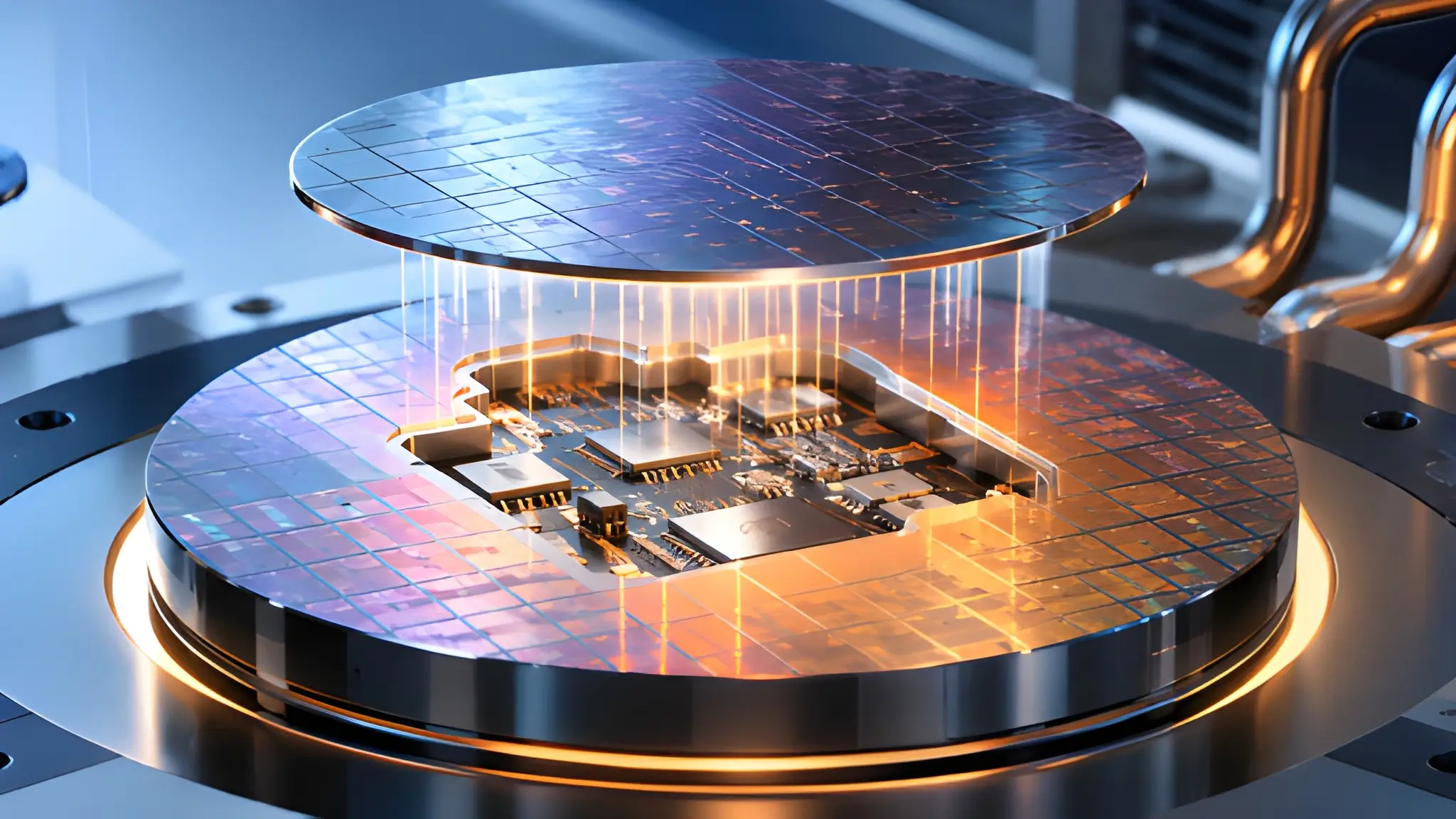
At the heart of EPP is a change in where packaging ends and semiconductor integration begins. Ramanathan explained that on a basic level, EPP works by taking a silicon wafer, making a cavity inside it, and then taking the die and putting it into the cavity. By using the wafer as the package, silicon, silicon carbide, and vertical gallium nitride can then be “seamlessly” interconnected within a “highly integrated wafer-level architecture.” That design allows different semiconductor technologies to operate within a common physical structure while reducing the separation between the device and its package.
EPP can embed FETs, drivers and controllers together inside one package, giving engineers a common platform for electrical, thermal and mechanical optimization. In an early EPP-based solid-state circuit-breaker design, onsemi said the solution was approximately 50% smaller and 20% cooler than existing designs. The company’s broader EPP architecture can support multiple semiconductor technologies, including silicon, silicon carbide and gallium nitride. Meanwhile, onsemi says its architecture can deliver up to 3-to-5 times higher power density than current solutions, while its EPP technology page cites up to four times improved power density depending on the implementation.

Manufacturing Strategy Anchors the Platform
The significance of EPP extends beyond the package itself because onsemi intends to build the architecture around established semiconductor manufacturing capabilities. The platform uses the company’s standard 12-inch silicon wafer manufacturing infrastructure, alongside mature design tools, wafer-level manufacturing and simulation capabilities. That gives onsemi a route to apply semiconductor manufacturing precision to power-system integration instead of relying entirely on conventional power-module approaches. The company says this integration can reduce development complexity while allowing electrical, thermal and mechanical characteristics to be optimized together.
“By reducing packaging overhead and using the full EPP footprint to conduct heat, EPP can support more compact power systems, improve thermal management and enable greater power density in AI infrastructure,” the company said in a statement. That proposition matters as AI systems push power conversion and delivery hardware closer to the same density constraints facing compute components. However, higher density does not remove the underlying challenge of managing heat and electrical losses; it makes the coordination between those elements more important. onsemi’s architecture attempts to address that problem at the package and system-design level rather than after the hardware has already been assembled.
Subaru Partnership Gives EPP an Early Customer
onsemi has already brought Subaru into the EPP development process, giving the automaker early access to engineering samples, simulation models and technical expertise. Subaru will evaluate the technology for future electrified-vehicle architectures, making the engagement an important test of EPP beyond data-center power systems. onsemi said the collaboration will provide customer feedback as it continues developing the platform for different power architectures. The companies described the engagement as an evaluation of next-generation power integration rather than a production deployment.
Ramanathan said onsemi is working with customers in both industrial and AI data-center markets, although the company has not publicly identified those partners. “We have shown [these customers] what the technology can do, and we’re working towards getting this product into revenue in the 2027 time frame, so we’re sampling our customers this year,” Ramanathan said. “The expectation is that in Q1, this technology will be qualified, and then made generally available for any of our customers to take to market.” onsemi separately says EPP will begin sampling with strategic customers and ecosystem participants across automotive and AI applications in 2026.
Power Delivery Moves Into the AI Bottleneck
The larger implication for AI infrastructure is that power density is becoming a system-level engineering problem rather than a specification attached to an individual chip. More compute per rack requires more electricity, but that electricity must move through power conversion, distribution and thermal-management hardware without consuming the physical space needed for compute. EPP represents onsemi’s attempt to compress those layers into a more integrated architecture. If customers adopt the approach at scale, the competitive question will shift from simply supplying more power to delivering that power within tighter electrical, thermal and mechanical constraints.