
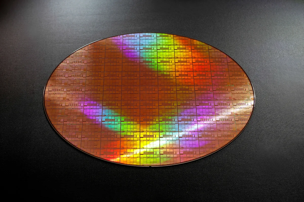
Prototypes of 2nm Gate All Around Transistors on Silicon Wafer; Source- Rapidus
Rapidus Corporation announced that prototyping has started for its 2nm gate-all-around (GAA) transistor structure at Rapidus’ Innovative Integration for Manufacturing (IIM-1) foundry. The prototype wafers also started to obtain their electrical characteristics.
Rapidus’ new IIM-1 foundry represents a significant advancement over the traditional foundry model. The company is re-imagining how semiconductor factories should think, learn, adapt and optimize processes in real time through cutting-edge methods and technology including:
Fully single-wafer front-end processing: In a single-wafer process, adjustments can be made to a single wafer, inspected and if successful, applied to all subsequent wafers. Single wafer captures more data, enabling AI models to be trained to improve wafer production and increase yields. Rapidus is one of the first companies that will commercialize fully single-wafer processing, which is central to its Rapid and Unified Manufacturing Service (RUMs).
Extreme Ultraviolet (EUV) lithography: EUV lithography is one of the key technologies for realizing 2nm semiconductors. An advanced lithography process is critical for forming the 2nm generation GAA structure. Rapidus is the first company to install advanced EUV machinery in Japan. Additionally on April 1, 2025, the company successfully completed EUV exposure, approximately three months after the equipment was delivered in December 2024.
At a press conference in Chitose, Rapidus President Atsuyoshi Koike announced that the company has reached “a major milestone” in its pursuit to begin mass production of 2-nanometer chips by 2027. (A nanometer is one-billionth of a meter.)
“Today marks a significant chapter in history,” echoed Hokkaido Governor Naomichi Suzuki.


