
Artificial intelligence computing continues to push semiconductor hardware toward unprecedented thermal densities, forcing engineers to reconsider how heat moves through silicon. Traditional cooling architectures were designed for processors whose heat generation spread across larger surfaces with lower localized density. AI accelerators now concentrate enormous switching activity inside specialized matrix engines and dense memory interfaces that generate intense heat at microscopic locations within the die. Thermal limits therefore increasingly constrain achievable clock speeds and sustained performance in high-end computing systems. Electrical scaling still progresses through packaging innovation and heterogeneous integration even as transistor miniaturization slows. These developments place thermal engineering at the center of modern processor design rather than treating cooling as an external afterthought.
Modern AI processors combine multiple chiplets, high-bandwidth memory stacks, and advanced interconnect fabrics inside tightly integrated packages. Each layer introduces additional electrical interfaces, bonding materials, and structural components that heat must traverse before reaching a cooling surface. Thermal resistance therefore accumulates across many boundaries within the package stack, which limits how efficiently conventional cold plates remove heat. Designers increasingly confront a scenario where transistor activity produces thermal flux faster than external cooling interfaces can extract it. Semiconductor roadmaps have consequently shifted attention toward cooling techniques that operate closer to the heat source itself. Engineers now explore architectures where thermal transport becomes embedded directly within the silicon structure. That transition signals a fundamental shift in how chips may manage energy in the coming generation of AI infrastructure.
Thermal Density as the Hidden Constraint in Compute Scaling
Chip designers historically prioritized transistor density, switching speed, and interconnect bandwidth when optimizing processors for performance. Thermal considerations often appeared later in the design process because air cooling or external liquid cooling provided adequate headroom for previous generations of hardware. AI accelerators changed this balance by concentrating arithmetic throughput into specialized execution units that operate continuously during training workloads. Sustained switching activity creates localized heat flux that spreads unevenly across the silicon surface. Conventional heat spreaders struggle to distribute that thermal energy evenly before it reaches the cooling interface. Engineers therefore encounter temperature gradients inside the die that influence reliability, performance stability, and power efficiency. Such conditions have gradually transformed thermal management into a first-order constraint for advanced computing systems.
Localized hotspots represent one of the most challenging aspects of thermal management in AI processors. Certain compute blocks activate more intensely than surrounding circuitry depending on the structure of the neural network workload. Those regions experience rapid temperature rises that can trigger throttling mechanisms or long-term material stress inside the package. External cooling solutions generally remove heat uniformly across the processor surface even though the underlying heat distribution remains uneven. Thermal engineers therefore search for techniques that deliver targeted cooling exactly where the highest heat flux occurs. Microfluidic channel networks embedded near active transistor layers provide one potential solution to this imbalance. Cooling pathways can be shaped to follow the actual heat generation patterns across the silicon die.
The emerging challenge resembles a physical barrier often described as a thermal wall. Transistors may continue to switch faster and compute units may expand in number, yet heat removal ultimately limits how much power the silicon can dissipate safely. Traditional packaging materials such as solder bumps, thermal interface compounds, and heat spreaders introduce unavoidable thermal resistance between the chip and the cooling fluid. Engineers cannot reduce those layers indefinitely without compromising electrical reliability or structural integrity. The result is a gradual bottleneck where additional computing capability becomes difficult to sustain thermally. Direct liquid cooling integrated inside the chip therefore attracts attention as a path around this barrier. Such approaches shorten the distance between the heat source and the coolant interface dramatically.
Why Conventional Cold Plates Are Reaching Their Limits
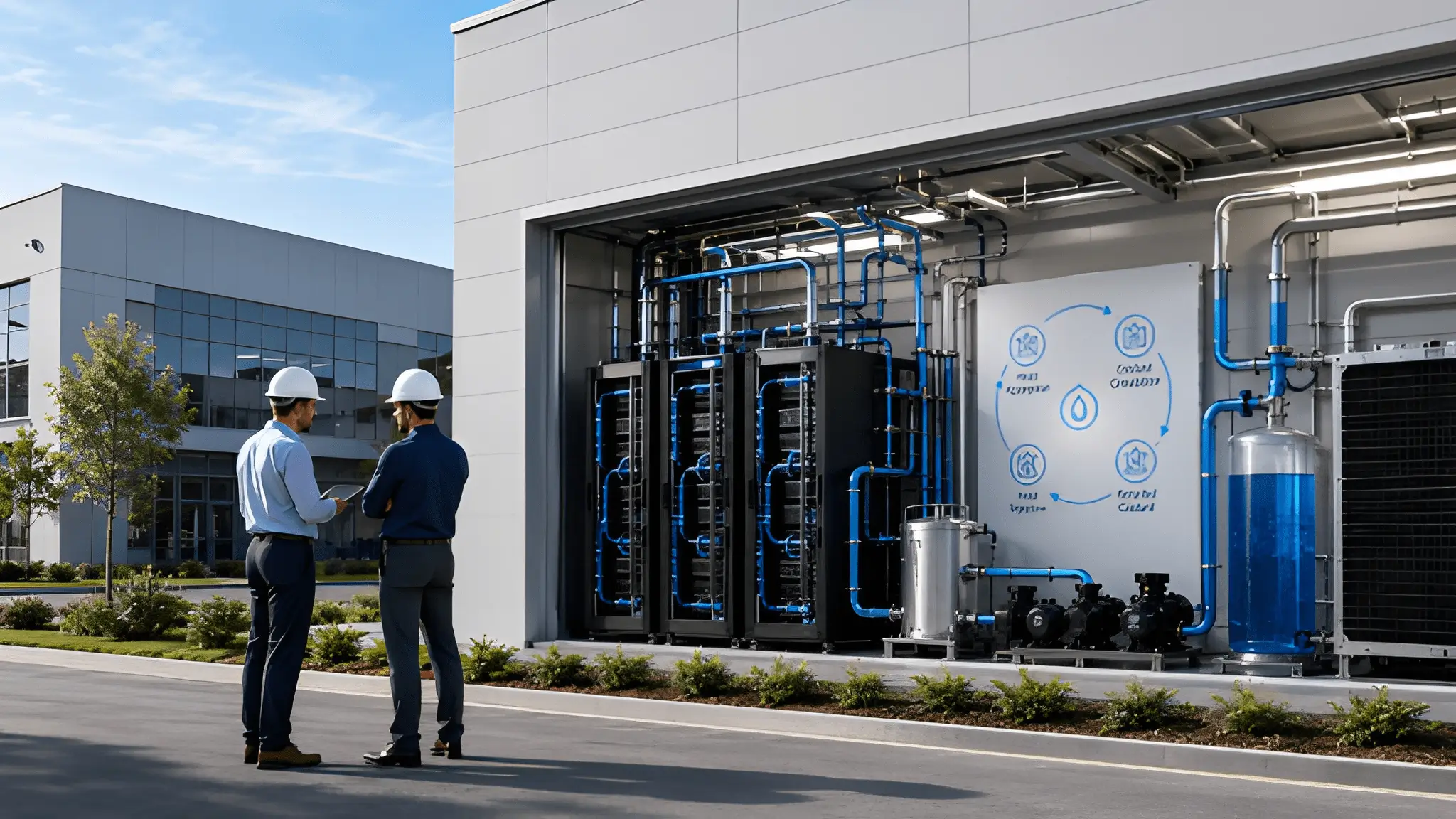
Cold plate liquid cooling has become a widely deployed solution for high-performance processors and GPU clusters in modern data centers. In this approach, a metal plate containing fluid channels sits on top of the processor package while coolant circulates through internal passages. Heat flows from the silicon die into a heat spreader and then into the cold plate before reaching the circulating liquid. The process works effectively when thermal loads remain within the capacity of these interfaces. However, each additional material layer introduces thermal resistance that slows the transfer of heat from the transistor layer to the coolant. AI accelerators with extremely dense power distribution now expose the limitations of that multi-layer pathway. Engineers increasingly recognize that external cooling surfaces alone may not provide sufficient proximity to the heat source.
The internal architecture of advanced processor packages compounds this challenge. High-bandwidth memory stacks and silicon interposers often surround the compute die to enable massive data throughput between components. These structures create additional mechanical and thermal boundaries between the die and the external cooling plate. Heat must propagate laterally through these materials before reaching the coolant interface. Such lateral spreading can increase temperature gradients across the die and reduce overall cooling efficiency. Designers therefore look for methods that intercept thermal energy earlier in its path. Embedded microfluidic cooling channels offer one such interception point directly within the silicon substrate.
Thermal interface materials play a crucial role in conventional cooling assemblies, yet they also introduce unavoidable inefficiencies. Engineers apply these compounds between the chip surface and the heat spreader to improve contact and reduce microscopic air gaps. Even with advanced materials, the interface still represents a thermal barrier that limits the rate of heat transfer. Repeated heating cycles may also alter the mechanical properties of these compounds over time. Reliability considerations therefore constrain how thin or aggressive such interfaces can become. Embedded cooling architectures aim to eliminate several of these intermediate layers altogether. The closer the coolant moves toward the transistor layer, the less thermal resistance the system accumulates.
External cooling systems also struggle to respond dynamically to rapidly changing heat patterns across modern processors. Workloads often shift computational intensity between different regions of the die depending on the algorithm. A cold plate typically distributes coolant evenly across its internal channels regardless of the instantaneous heat distribution below. Engineers therefore investigate cooling systems that can adapt their flow patterns according to thermal activity within the chip. Microfluidic channel networks etched directly into silicon provide the geometric flexibility needed to shape coolant pathways precisely. Those channels can be arranged to focus cooling capacity near the most thermally active circuits. Such adaptability becomes increasingly valuable as chip architectures grow more heterogeneous.
Enter Microfluidic Cooling: Channels Carved Inside Silicon
Microfluidic cooling represents a radical departure from traditional processor thermal management strategies. Instead of removing heat after it leaves the chip surface, engineers create microscopic fluid channels directly inside the silicon substrate. Coolant flows through these channels while the surrounding silicon transfers heat directly into the circulating liquid. The process drastically shortens the conduction path between the transistor layer and the cooling medium. Researchers have demonstrated several fabrication approaches that integrate these channels using techniques compatible with semiconductor manufacturing. Silicon etching processes form narrow trenches that later become sealed microchannels capable of carrying liquid coolant. This architecture effectively turns the chip itself into part of the cooling system.
Microchannels embedded within the silicon substrate allow heat extraction to occur extremely close to active transistor regions. That proximity reduces the temperature difference required to drive thermal transfer from the die to the coolant. Engineers often design these channels with dimensions measured in tens or hundreds of micrometers. Such scales increase the surface area between the liquid and the silicon walls, improving convective heat transfer efficiency. Fluid distribution networks then connect these channels to inlet and outlet ports integrated into the chip package. The result resembles a miniature plumbing system etched into the processor itself.
Fabrication techniques for microfluidic cooling borrow concepts from both semiconductor processing and microelectromechanical systems engineering. Engineers typically begin by etching channels into the backside of the silicon wafer using deep reactive ion etching or similar methods. A sealing layer then encloses the channels to form a watertight network capable of carrying coolant under pressure. Fluidic vias connect the microchannels to external tubing or package-level manifolds. Electrical interconnects continue to operate independently of the cooling network. Researchers have demonstrated prototypes where fluidic and electrical connections integrate within the same packaging architecture.
Microfluidic cooling systems also support advanced heat transfer modes that extend beyond simple liquid flow. Some experimental designs use two-phase cooling where the coolant undergoes controlled phase change within the microchannels. When the liquid absorbs heat from the silicon, it partially vaporizes and carries thermal energy away through latent heat transfer. Engineers carefully design channel geometry and pressure conditions to manage this process without causing flow instability. Two-phase microfluidic cooling has demonstrated promising thermal performance in experimental processor modules. These demonstrations suggest that chip-integrated cooling could support the power densities expected in future AI hardware.
Designing Fluid Pathways Inside Semiconductor Wafers
Embedding coolant pathways within silicon wafers introduces a new design dimension that merges semiconductor engineering with fluid mechanics. Engineers must determine how coolant flows through microchannels while preserving electrical isolation, structural integrity, and manufacturability. Silicon wafers remain fragile structures that must survive lithography, bonding, packaging, and thermal cycling throughout their lifecycle. Introducing fluid passages within this material therefore requires careful structural planning to prevent mechanical stress or fracture during fabrication and operation. Designers must also ensure that microchannels do not interfere with through-silicon vias or electrical routing layers that enable communication between chip components. Thermal and fluid simulations guide these layouts so that coolant pathways intercept heat efficiently without compromising the electrical architecture.
Channel geometry strongly influences how effectively coolant removes heat from the silicon substrate. Engineers experiment with serpentine pathways, parallel microchannel arrays, and branching networks that distribute fluid evenly across the chip surface. Narrow channels increase the surface area available for heat transfer, yet extremely small passages increase flow resistance and require higher pumping pressure. Designers therefore balance thermal efficiency with hydraulic feasibility when selecting channel dimensions. Computational fluid dynamics simulations help engineers predict how liquid moves through these microscopic networks under different conditions. Such models also identify potential stagnation zones where coolant flow might weaken. Preventing such zones remains critical because localized flow reduction could allow thermal hotspots to develop within the silicon structure.
Thermal engineers must also consider how fluid pathways align with the distribution of heat sources on the die. AI accelerators contain compute clusters, memory controllers, and interconnect fabrics that generate heat unevenly across the silicon surface. Uniform channel spacing might not provide optimal cooling for such heterogeneous architectures. Designers therefore map thermal profiles generated by representative workloads and then align microchannels accordingly. This targeted alignment ensures that coolant passes directly beneath the most thermally active circuits. Such design strategies help maximize cooling efficiency without requiring excessive coolant flow across the entire chip. Precision alignment between microfluidic channels and compute hotspots therefore becomes an important element of future chip design workflows.
Engineers must also develop methods for sealing microchannels once they have been etched into the silicon wafer. A thin bonding layer typically covers the channel network and creates an enclosed pathway capable of carrying coolant. Bonding techniques may involve silicon-to-silicon fusion bonding, glass capping layers, or specialized wafer bonding processes. Each approach must withstand thermal expansion, pressure fluctuations, and mechanical vibration throughout the chip’s operational lifetime. Leakage cannot be tolerated within semiconductor packages because even microscopic fluid escape could damage sensitive circuitry. Packaging engineers therefore devote considerable effort to ensuring hermetic sealing of these embedded cooling networks. Such sealing methods represent one of the most critical engineering challenges in practical on-die liquid cooling systems.
Integrating Fluidic Design With Chip Layout
The introduction of fluidic structures within silicon forces semiconductor design teams to collaborate across disciplines that rarely intersected previously. Chip architects must now consider how coolant pathways influence the physical layout of compute blocks and interconnect networks. Routing electrical signals, distributing power, and arranging fluid channels must occur simultaneously rather than sequentially. Computer-aided design tools are gradually evolving to support these integrated workflows. Thermal simulations feed directly into layout optimization algorithms that determine the placement of microchannels relative to heat-generating circuits. Engineers therefore treat cooling structures as intrinsic elements of the chip floorplan rather than external attachments. Such integration reflects the growing importance of thermal management in high-performance computing hardware.
Another factor shaping microfluidic design involves the physical interface between the chip and external coolant supply lines. Fluid must enter and exit the embedded channel network through connections integrated into the package substrate or interposer. Engineers therefore design fluidic ports that align precisely with the microchannel inlet structures etched within the silicon. These connections must maintain reliable seals while accommodating pressure variations and thermal expansion. Packaging technologies such as silicon interposers or micro-manifold layers help distribute coolant evenly to multiple chips in a module. Integration at this level requires precise alignment during assembly. The interface between the chip and the external cooling loop thus becomes an important component of the overall microfluidic architecture.
Hotspot-Aware Cooling Architectures for AI Workloads
Artificial intelligence workloads produce dynamic patterns of computation that differ significantly from traditional processor activity. Neural network training often activates certain compute clusters continuously while other parts of the chip remain relatively idle. This uneven utilization leads to thermal hotspots that emerge in specific regions of the silicon die. Conventional cooling systems remove heat uniformly across the processor surface regardless of these localized variations. Microfluidic cooling enables engineers to address this challenge by shaping coolant pathways according to actual heat generation patterns. Cooling channels can run directly beneath tensor compute units or memory interface blocks that generate the most thermal energy. Such hotspot-aware designs improve temperature uniformity across the chip while preventing localized overheating.
Thermal sensors embedded within the processor can further enhance the responsiveness of these cooling systems. Many modern processors already include temperature monitoring circuits that report real-time thermal conditions across different regions of the die. When combined with microfluidic cooling networks, these sensors can inform adaptive flow control systems. Coolant flow rates may increase in regions experiencing heavier computational load. Such adaptive behavior requires sophisticated control systems capable of regulating micro-scale fluid movement with high precision. Researchers continue to investigate feedback mechanisms that connect thermal monitoring with fluidic control loops. These approaches could eventually allow chips to regulate their own cooling behavior dynamically.
Workload-aware cooling architectures also influence how software interacts with hardware resources. Scheduling algorithms that distribute neural network workloads across the chip could account for thermal conditions in real time. When a particular compute cluster approaches its thermal threshold, workloads might shift temporarily to cooler regions of the die. Microfluidic cooling can complement such strategies by concentrating fluid flow in areas experiencing heavy computational demand. This coordination between software scheduling and embedded cooling infrastructure represents an emerging area of research. Engineers view such integration as a way to maintain sustained performance while avoiding temperature-induced throttling. The interaction between computing workloads and cooling architecture therefore becomes increasingly interconnected in future AI processors.
Another advantage of hotspot-aware cooling lies in its ability to reduce thermal gradients within the silicon structure. Large temperature differences between regions of the chip can cause mechanical stress due to uneven thermal expansion. Over time, these stresses may affect solder joints, interconnect structures, or bonding layers within the package. Targeted cooling reduces the magnitude of these gradients by stabilizing temperatures across the die. This stabilization contributes to improved reliability and longer component lifespan. Engineers therefore view microfluidic cooling not only as a performance solution but also as a structural reliability strategy. Managing thermal gradients has become a crucial aspect of advanced semiconductor packaging.
Integrating Cooling With 3D Stacked Chiplet Architectures
Three-dimensional chip stacking has become a key strategy for improving computing performance without relying solely on transistor scaling. Engineers stack multiple silicon layers vertically to reduce communication distance between logic units and memory components. High-bandwidth memory modules already employ stacked architectures that place several memory dies directly above one another. This configuration dramatically increases data throughput while minimizing signal delay. However, stacking silicon layers also concentrates heat within a confined vertical space. Thermal energy generated by lower layers must travel through multiple dies before reaching a cooling interface. Such conditions create significant challenges for conventional cooling methods.
Embedded liquid cooling offers a potential solution to the thermal constraints of stacked chip architectures. Engineers can integrate microchannels between stacked layers or within intermediate silicon interposers. Coolant flowing through these channels can remove heat from multiple layers simultaneously. This approach reduces the thermal resistance associated with vertical heat conduction through stacked dies. Researchers have demonstrated experimental packages where microfluidic networks operate between memory and logic layers. These structures intercept heat before it accumulates within the stack. Such architectures may become increasingly important as vertical chip integration continues to expand.
Fluid distribution becomes more complex in vertically stacked chip systems. Coolant pathways must reach multiple layers while maintaining consistent flow rates across the entire structure. Engineers may use micro-manifolds integrated into interposer layers to distribute coolant evenly between stacks. These manifolds function similarly to plumbing distribution systems but operate on microscopic scales within semiconductor packages. Precise control of pressure and flow ensures that coolant reaches all regions of the stack effectively. Designers must also avoid introducing vibrations or mechanical stresses that could affect electrical interconnects. Integration between fluidic systems and high-density electrical connections therefore requires careful engineering.
Thermal simulation plays a critical role in developing stacked chip cooling architectures. Engineers analyze how heat propagates through each layer of the stack under realistic computational workloads. Simulation tools evaluate how microchannel placement influences heat removal efficiency across the structure. Such models help determine optimal coolant flow paths that minimize temperature gradients within the stack. These simulations also assess mechanical stresses introduced by thermal expansion and fluid pressure. Through iterative modeling, engineers refine designs before committing them to fabrication. Such methods accelerate the development of integrated cooling solutions for complex three-dimensional processor architectures.
Pumping Liquids Through Chips: The Microfluidic Flow Challenge
Circulating liquid through microscopic channels inside semiconductor structures introduces a complex fluid dynamics problem that differs significantly from conventional cooling loops. The diameter of microchannels etched into silicon often approaches scales where viscous forces dominate the behavior of moving fluids. Engineers must therefore design pumping systems capable of maintaining stable flow without introducing excessive pressure within the chip package. Even small pressure variations can influence the structural stability of thin silicon layers surrounding the microchannels. Flow distribution also becomes sensitive to minute differences in channel geometry or surface roughness created during fabrication. Such conditions demand precise engineering to maintain uniform coolant circulation throughout the chip.
Fluid pressure remains one of the central constraints in microfluidic cooling architectures. The pumping system must overcome resistance created by narrow channels while preventing mechanical stress on the silicon substrate. Excessive pressure could distort bonding layers or compromise sealing interfaces that enclose the coolant network. Engineers therefore analyze pressure drop characteristics across the microchannel network during the design phase. Computational models help estimate how coolant velocity changes along the channel pathways. These simulations guide adjustments in channel width, branching structure, and inlet distribution. The goal involves achieving consistent flow across the chip while maintaining safe pressure levels within the silicon package.
Another engineering consideration involves the selection of pumping technologies that can operate at extremely small flow scales. Traditional pumps designed for industrial liquid cooling loops may not provide the precision required for microfluidic circulation. Engineers investigate miniature pumping systems such as piezoelectric pumps or micro-scale mechanical pumps integrated into cooling assemblies. These devices can generate controlled fluid motion suitable for delicate microchannel networks. Their compact form also allows integration within server modules or processor packages. Stable pumping behavior remains essential because fluctuations in flow rate could produce uneven cooling across the chip. Consistent coolant circulation therefore forms a fundamental requirement for reliable on-die liquid cooling systems.
Flow stability inside microchannels also depends on the physical properties of the coolant itself. Viscosity determines how easily the fluid travels through narrow passages, while density influences pressure characteristics throughout the network. Engineers must evaluate how these properties interact with the geometry of the etched channels. Channel walls created during silicon etching may exhibit microscopic roughness that alters fluid behavior. Such effects become increasingly significant at the micro-scale because the fluid interacts closely with the channel surface. Careful control of fabrication processes therefore contributes directly to the hydraulic performance of the cooling system. Understanding these interactions helps engineers design microfluidic cooling networks capable of stable long-term operation.
Flow Control and Thermal Stability
Effective microfluidic cooling systems must regulate coolant distribution with high precision to maintain stable thermal conditions across the processor. Sensors integrated into the cooling loop can measure pressure, temperature, and flow rate at various points within the system. These measurements allow control circuits to adjust pump speed or valve settings in response to changing thermal conditions. Dynamic regulation helps prevent situations where one region of the chip receives insufficient coolant flow. Control algorithms may also compensate for variations caused by workload fluctuations during AI training or inference tasks. Such active regulation improves the resilience of embedded cooling architectures. Feedback-driven flow control therefore represents a critical component of practical on-die cooling systems.
Maintaining stable thermal behavior requires careful coordination between the cooling system and the electrical power characteristics of the chip. Power distribution networks may cause certain compute clusters to activate more frequently than others depending on the computational workload. When thermal monitoring detects rising temperatures in these areas, flow control mechanisms can direct additional coolant through nearby channels. Such targeted cooling reduces temperature gradients that might otherwise appear across the silicon surface. Engineers design control systems that respond quickly to these changes without introducing oscillations in the cooling loop. Stability in both the electrical and fluidic domains therefore becomes essential. Integration between thermal monitoring and fluid regulation enables the chip to sustain high performance under demanding workloads.
Materials Science Behind On-Die Cooling
Embedding liquid within semiconductor packages introduces significant materials engineering challenges. Silicon alone cannot serve as the only structural material because the cooling system must resist corrosion, maintain sealing integrity, and tolerate thermal cycling during operation. Engineers therefore evaluate combinations of silicon, glass, metals, and advanced polymers when designing microfluidic cooling structures. Each material must provide compatibility with semiconductor fabrication processes while also interacting safely with the chosen coolant. Mechanical strength becomes critical because the cooling network must endure pressure variations as fluid circulates through microscopic channels. Materials selection thus influences both the reliability and performance of the cooling architecture.
Bonding layers that seal microchannels require particular attention from materials scientists. These layers must create hermetic barriers that prevent coolant leakage over long operational lifetimes. Silicon-to-silicon bonding techniques offer strong structural integrity because the bonding interface forms a continuous crystalline connection. Glass capping layers provide another approach because they can bond securely to silicon while remaining chemically stable in contact with many fluids. Engineers must ensure that bonding layers maintain adhesion even under repeated thermal expansion cycles. Variations in thermal expansion coefficients between materials could introduce mechanical stress if not carefully managed. Reliable bonding technology therefore represents a cornerstone of practical on-die liquid cooling systems.
Surface chemistry also plays a major role in determining the long-term stability of microfluidic cooling channels. Coolants flowing through silicon channels may interact with the channel walls at the molecular level. These interactions can influence corrosion behavior, deposition of impurities, or changes in surface roughness over time. Engineers often apply protective coatings to channel surfaces in order to prevent chemical degradation. Thin dielectric layers may also provide electrical insulation between the coolant and nearby electronic structures. These coatings must remain uniform and defect-free throughout the entire channel network. Advances in thin-film deposition techniques therefore contribute significantly to the viability of embedded cooling systems.
Material compatibility must also extend to the external components that connect the chip to the larger cooling loop. Tubing, connectors, and manifold structures must interact safely with the same coolant circulating inside the microchannels. If incompatible materials are used, chemical reactions could introduce contaminants into the fluid. Such contamination might eventually clog narrow microchannels within the chip. Engineers therefore evaluate the entire cooling loop as a unified materials system rather than focusing only on the chip itself. This holistic approach helps ensure that all components maintain stable behavior during extended operation. Materials science thus underpins the reliability of microfluidic cooling across the entire infrastructure stack.
Coolants for the Silicon Era: Beyond Water
Selecting the appropriate coolant represents another critical decision in the development of on-die liquid cooling architectures. Water has long served as an effective heat transfer fluid in many industrial cooling systems because of its favorable thermal properties. However, the presence of water near electronic components introduces potential electrical and chemical risks. Engineers must ensure that the coolant cannot conduct electricity in the event of a leak or contact with exposed circuitry. For this reason, researchers investigate alternative fluids that combine strong thermal performance with electrical insulation properties. Such fluids enable safe operation even when coolant flows directly within semiconductor structures.
Dielectric fluids provide one promising category of coolant for embedded chip cooling systems. These liquids exhibit extremely low electrical conductivity while still offering reasonable thermal capacity. Because they do not conduct electricity, dielectric fluids reduce the risk of short circuits if accidental contact occurs with electronic components. Engineers have already deployed similar fluids in certain immersion cooling systems for data center hardware. Adapting them for microfluidic channels inside silicon packages requires additional evaluation of viscosity and chemical compatibility. The fluid must flow easily through narrow channels while remaining stable under long-term exposure to silicon surfaces. Careful testing therefore accompanies the selection of dielectric coolants for semiconductor applications.
Nanofluids represent another area of research aimed at improving the heat transfer characteristics of cooling liquids. These fluids contain microscopic particles suspended within a base liquid to enhance thermal conductivity. The particles may consist of metals, metal oxides, or carbon-based materials engineered to interact efficiently with heat energy. When properly formulated, nanofluids can increase the rate at which heat moves from the silicon walls into the circulating liquid. However, engineers must ensure that suspended particles remain stable and do not accumulate inside microchannels. Even slight deposition within narrow passages could obstruct fluid flow. Research therefore continues to evaluate how nanofluids behave within micro-scale cooling networks.
Fluid stability under varying temperature conditions also becomes important for semiconductor cooling systems. AI processors often experience significant temperature fluctuations as workloads change during operation. The coolant must maintain consistent physical properties across this temperature range. Changes in viscosity or density could alter flow characteristics within the microchannel network. Engineers therefore conduct extensive testing to ensure that candidate fluids behave predictably under thermal cycling. The coolant must also resist evaporation or chemical breakdown during prolonged operation. Selecting the correct fluid thus involves balancing thermal performance, chemical stability, and compatibility with microfluidic structures.
Manufacturing the Liquid-Cooled Processor
Integrating cooling channels directly into semiconductor wafers requires adjustments to established chip manufacturing workflows. Conventional fabrication processes focus on building transistor layers, interconnect networks, and protective passivation structures on the surface of the silicon wafer. On-die liquid cooling introduces additional steps that create microchannel structures within the wafer substrate itself. Engineers must incorporate these processes without disrupting the precision required for advanced transistor fabrication. Deep reactive ion etching often forms the initial microchannel network on the backside of the wafer after front-end device fabrication has completed. This stage allows cooling structures to develop without interfering with the delicate transistor layers near the top surface. Process integration therefore becomes an essential challenge in the evolution of liquid-cooled processors.
Wafer bonding technology plays a crucial role in sealing the etched microchannels and transforming them into functional fluid pathways. After channel structures form within the silicon substrate, engineers attach a capping layer that encloses the fluid network. Silicon-to-silicon bonding often provides the strongest structural connection because the bonded interface behaves similarly to the surrounding crystal lattice. Alternative bonding techniques may involve glass or polymer layers that provide flexibility in certain packaging scenarios. Regardless of the approach, the bonding interface must remain perfectly sealed throughout the lifetime of the chip. Even microscopic imperfections could allow coolant leakage or introduce contaminants into the microchannel system. Manufacturing teams therefore develop stringent inspection methods to verify the integrity of every bonded wafer.
After sealing the microchannels, additional processing steps integrate fluidic connections into the chip package. These connections allow coolant to enter and exit the microfluidic network once the processor is installed within a server system. Engineers may use through-silicon vias or dedicated fluidic ports positioned near the edges of the die. Packaging substrates then route the fluid toward external tubing connected to the cooling infrastructure of the data center. This integration must occur alongside traditional electrical connections that deliver power and high-speed data signals to the processor. Maintaining alignment between fluidic ports and packaging interfaces requires precise assembly techniques. Advanced semiconductor packaging therefore becomes tightly coupled with the implementation of on-die cooling technologies.
Process compatibility remains another important factor in manufacturing liquid-cooled chips. Semiconductor fabrication lines operate with extremely tight contamination controls to protect sensitive device layers. Introducing fluidic structures into the wafer must not compromise these cleanroom conditions. Engineers therefore ensure that channel etching, bonding materials, and sealing processes do not release particles or chemicals that could affect transistor reliability. Manufacturing research continues to evaluate how these additional steps can integrate smoothly into large-scale production lines. Prototype demonstrations have already shown that microfluidic cooling can coexist with advanced semiconductor processes. Continued refinement of these techniques will determine whether such designs become practical for commercial AI processors.
Reliability Risks When Liquids Meet Silicon
The presence of liquid coolant inside semiconductor packages introduces reliability concerns that engineers must address before widespread deployment becomes feasible. Silicon devices operate within tightly controlled environments where contamination or moisture exposure can damage delicate electronic structures. Introducing fluidic channels within the chip therefore raises questions about long-term stability and failure mechanisms. Even small leaks within the microchannel network could expose internal circuitry to liquid. Such events might cause corrosion or electrical interference that compromises processor functionality. Engineers therefore design multiple layers of protection to minimize the possibility of coolant escape. Reliability analysis plays a central role in the development of on-die cooling technologies.
Clogging represents another potential reliability issue in microfluidic cooling systems. Because the channels inside silicon are extremely narrow, even tiny particles or chemical deposits could obstruct fluid flow. Reduced flow would decrease cooling performance and potentially allow temperatures to rise in certain regions of the chip. Engineers therefore implement filtration systems within the external cooling loop to remove contaminants before coolant enters the processor. Fluid chemistry must also remain stable so that deposits do not accumulate along the channel walls over time. Regular monitoring of coolant quality helps maintain consistent performance throughout the lifespan of the hardware. Preventing microchannel blockage remains an important aspect of operational reliability.
Mechanical stress generated by thermal expansion can also influence the durability of embedded cooling structures. Silicon, bonding materials, and coolant fluids may expand at different rates when temperature changes occur during operation. These differences can create mechanical forces along channel walls or bonding interfaces. Engineers therefore select materials with compatible thermal expansion properties to minimize such stresses. Finite element simulations help evaluate how the cooling structure responds during repeated heating and cooling cycles. These analyses guide improvements in channel geometry and bonding strategies. Careful materials engineering therefore contributes to the long-term reliability of liquid-cooled semiconductor devices.
Erosion of channel surfaces represents another phenomenon that engineers must consider. Continuous fluid movement across silicon surfaces could gradually alter the microscopic structure of the channel walls. Over long operational periods this erosion might influence flow characteristics or introduce particles into the coolant. Protective coatings applied during fabrication help shield the silicon surfaces from direct chemical interaction with the fluid. Researchers continue to investigate coating materials that maintain stability under both mechanical and thermal stress. Long-term testing of microfluidic cooling prototypes provides insight into how these systems behave during extended operation. Such testing remains essential before on-die liquid cooling can reach commercial deployment at scale.
Energy Efficiency Gains From Direct Silicon Heat Extraction
Removing heat directly from the silicon substrate changes the thermal dynamics of processor cooling systems in meaningful ways. Conventional cooling architectures rely on heat conduction through several intermediate layers before the thermal energy reaches a circulating fluid. Each layer adds resistance that slows the movement of heat away from the transistor region. Microfluidic cooling dramatically shortens this path by placing coolant channels close to the active silicon. The reduced thermal resistance allows heat to move more efficiently from the die into the cooling fluid. This improvement enables processors to maintain stable operating temperatures even under sustained computational workloads. Efficient heat extraction therefore supports consistent performance in high-density computing environments.
Improved thermal efficiency can influence how processors manage electrical power internally. When heat dissipates quickly from the transistor layer, the chip can operate closer to its intended performance envelope without triggering thermal protection mechanisms. This stability reduces the need for aggressive throttling during heavy workloads. Engineers therefore gain greater flexibility when designing power management algorithms for high-performance processors. The cooling system effectively becomes an enabling factor that allows the silicon to sustain higher utilization levels. Stable thermal behavior also contributes to predictable performance characteristics during large computational tasks. These benefits align closely with the requirements of modern AI infrastructure.
Direct heat extraction also improves temperature uniformity across the chip surface. Because coolant flows near the transistor layer, localized hotspots can dissipate thermal energy more quickly. This uniformity reduces the formation of large temperature gradients within the silicon die. Lower gradients help maintain mechanical stability across the package because different regions of the chip experience similar thermal expansion. Such stability contributes to improved reliability for solder joints, bonding layers, and interconnect structures. Engineers therefore view on-die cooling as a mechanism that benefits both performance and structural durability. Balanced thermal conditions represent an important goal in advanced processor design.
Another efficiency advantage arises at the system level within data center infrastructure. When processors dissipate heat more effectively at the chip level, the facility’s external cooling systems can operate under less strain. Servers may require lower airflow or reduced reliance on large heat exchangers because much of the thermal energy leaves the chip through liquid cooling loops. This shift can simplify the thermal architecture of high-density computing racks. Facility designers may gain additional flexibility when arranging compute clusters within data halls. Direct silicon cooling therefore influences not only chip performance but also the broader energy dynamics of computing facilities.
The Data Center Implications of On-Die Cooling
The adoption of on-die liquid cooling could reshape server architecture across future data center deployments. Current liquid-cooled servers typically attach cold plates to the surface of processors and route coolant through manifolds connected to rack-level distribution units. Embedded microfluidic cooling would move the primary heat extraction point directly into the chip package. This shift would change how server designers approach thermal management inside compute nodes. Fluid connections might interface directly with processor modules rather than external heat spreaders. Such changes would influence motherboard layouts, socket designs, and rack cooling infrastructure. Hardware architects therefore evaluate how microfluidic cooling integrates with existing server standards.
Rack density could also evolve as embedded cooling technology matures. AI infrastructure already concentrates large numbers of accelerators within tightly packed server systems. Effective chip-level cooling may allow these systems to operate with greater thermal stability even when compute density increases. Data center designers could place more processing capability within each rack without exceeding facility cooling limits. Liquid loops integrated directly into processors may connect to centralized coolant distribution networks throughout the data hall. This architecture resembles industrial cooling systems where fluid carries heat away from critical equipment. Embedded cooling technologies therefore align naturally with the liquid-centric cooling strategies emerging in hyperscale data centers.
Infrastructure planning must also consider maintenance procedures for hardware that contains internal cooling channels. Technicians responsible for server maintenance may need specialized procedures when replacing processors connected to liquid loops. Quick-disconnect fluid couplings and leak detection systems would likely become standard features of such systems. Data center operators already manage similar procedures for immersion cooling or direct-to-chip cooling installations. Extending these practices to on-die liquid cooling would represent a logical evolution rather than a completely new operational paradigm. Engineers therefore examine how serviceability can coexist with the precision required for microfluidic cooling systems. Operational practicality remains essential for adoption within large computing facilities.
Another implication involves the integration of cooling infrastructure with facility-level energy systems. Liquid cooling loops can transport heat away from processors more efficiently than traditional air-based systems. Data centers may route this thermal energy toward heat exchangers or energy reuse systems located elsewhere in the facility. Embedded chip cooling therefore contributes to broader strategies for thermal management across the entire computing environment. The chip, the server, and the facility cooling loop become interconnected components of a unified thermal architecture. Such integration reflects the increasing importance of thermal engineering in the design of high-performance computing infrastructure.
When Cooling Becomes Part of the Processor
Thermal management in advanced processors is gradually transitioning from an external engineering challenge into an intrinsic component of chip design. Microfluidic cooling channels etched into silicon substrates represent a significant step toward integrating cooling infrastructure directly within semiconductor devices. These architectures shorten the thermal path between heat-generating transistors and the circulating coolant responsible for removing that heat. By addressing thermal constraints at their source, engineers gain new flexibility when designing high-density computing hardware. On-die liquid cooling therefore reflects a broader shift toward co-design between thermal systems and electronic architectures. The processor increasingly becomes both a computing engine and a thermal management platform.
Advances in semiconductor fabrication, materials science, and microfluidic engineering continue to expand the feasibility of these embedded cooling systems. Researchers have already demonstrated prototypes that integrate fluid channels, sealing layers, and fluidic connectors within working processor modules. Ongoing development focuses on improving manufacturing compatibility and ensuring long-term reliability. Engineers must refine bonding techniques, channel geometries, and coolant formulations before such technologies can reach large-scale deployment. Despite these challenges, the direction of research suggests that thermal integration will play a greater role in future processor architectures. Cooling infrastructure may eventually appear alongside electrical interconnects as a fundamental element of chip design.
Future AI hardware will likely continue to push the boundaries of computational density and electrical power within semiconductor packages. As these systems evolve, the ability to remove heat efficiently from the silicon substrate will remain essential for sustaining performance. On-die liquid cooling offers a pathway toward meeting these demands by embedding fluidic heat extraction directly within the chip itself. This approach transforms cooling from an external accessory into a structural feature of the processor. Such integration may redefine how engineers approach the relationship between computation, materials, and energy flow inside modern hardware. The emerging frontier of on-die cooling therefore represents a pivotal development in the future of high-performance computing infrastructure.