Skip to content
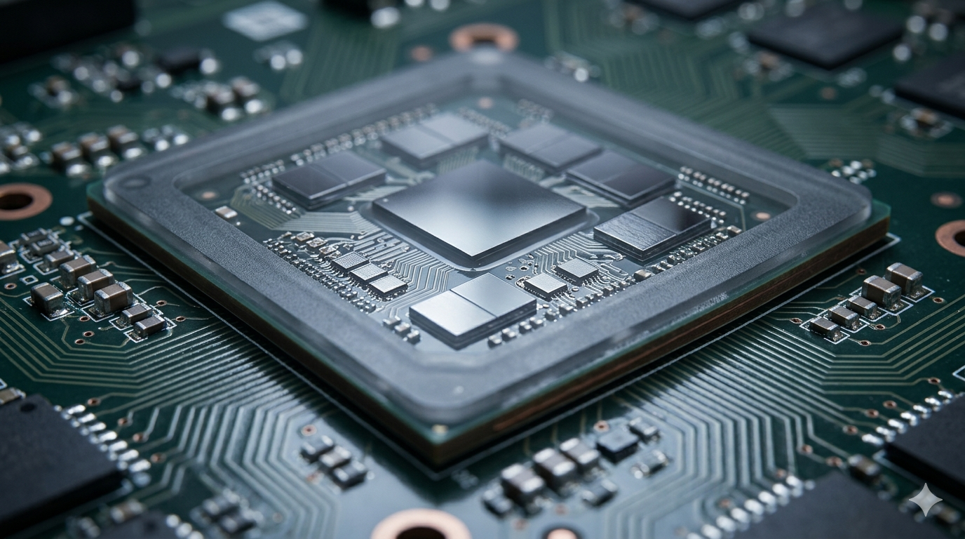
The monolithic chip, a single die performing all compute functions, dominated semiconductor design for decades. It was a workable model when transistor scaling continued to deliver predictable performance improvements at manageable cost. That model is now giving way to a fundamentally different approach. Chiplet architecture, which disaggregates compute, memory, and I/O functions across multiple smaller dies that communicate through high-speed interconnects, is becoming the default design paradigm for AI accelerators. The transition carries implications that extend well beyond semiconductor engineering, touching the economics of AI compute, the competitive dynamics among chip vendors, and the infrastructure requirements of the data centers that run these systems.

The shift is not happening because chiplets are technically superior in every dimension. They introduce integration complexity, interconnect latency, and packaging challenges that monolithic designs avoid. The reason chiplets are winning is more fundamental. The semiconductor manufacturing process nodes that deliver the most advanced compute performance are extraordinarily expensive to access and capacity-constrained. By disaggregating a design into smaller dies, each optimised for a specific function and manufactured on the most appropriate process node for that function, chiplet architectures allow designers to achieve system-level performance that a monolithic approach at equivalent total die area would cost far more to produce, if it could be manufactured reliably at all.
The Economics That Made Chiplets Inevitable
Manufacturing yield is the critical economic driver behind chiplet adoption. A larger die has more surface area, which means more opportunity for defects to land in the active circuitry. As die sizes have grown to accommodate the memory bandwidth, compute density, and I/O capacity that AI workloads demand, yield rates on monolithic designs have fallen in ways that make the per-chip economics progressively less attractive. A chiplet approach, breaking a large design into smaller dies, improves yield on each individual component because smaller dies have fewer defects per unit, and only the defective dies need to be discarded rather than entire assemblies.
The cost implications are significant at the scale at which AI accelerators are procured. When hyperscalers are ordering hundreds of thousands of GPU or accelerator units, even a modest improvement in manufacturing yield across that volume translates into substantial cost reduction. That calculation has driven the leading AI chip designers toward chiplet approaches even where the technical engineering challenges of high-speed die-to-die interconnects add design complexity that monolithic approaches avoid.
AMD’s move to chiplet architecture across its CPU and GPU product lines demonstrated the approach at commercial scale before the AI compute wave created the current urgency. The MI300 AI accelerator, which combines compute and memory chiplets in a single package, has achieved market traction at hyperscalers partly because its chiplet-based HBM memory integration delivers memory bandwidth that a monolithic design could not provide at competitive cost. NVIDIA’s own architecture has moved toward multi-die integration in the Blackwell generation, combining GPU and NVLink switch dies in a way that reflects the same underlying economic logic.
What Heterogeneous Integration Actually Means
The technical term for the broader trend that chiplets represent is heterogeneous integration. It describes the practice of combining dies manufactured on different process nodes, from different vendors, with different functional specialisations, into a single package that performs as a unified system. A modern AI accelerator might combine compute dies manufactured on TSMC’s most advanced 3nm or 2nm processes with memory dies that use different, more cost-effective process nodes optimised for density rather than raw transistor performance.

That combination allows designers to put the most expensive advanced process node budget where it creates the most value, in the logic circuits executing AI compute operations, while using lower-cost processes for functions where advanced node performance is not the primary requirement. The result is a package whose performance-per-dollar exceeds what a fully monolithic approach at the same total transistor count would deliver.
Beyond GPUs, the hidden architecture powering the AI revolution includes the interconnect fabrics, memory hierarchies, and packaging innovations that heterogeneous integration depends on. The die-to-die interconnect is the critical enabling technology in chiplet systems. If the communication bandwidth between chiplets is insufficient, or if the latency is too high, the performance advantages of disaggregation are lost to communication overhead. Standards like Universal Chiplet Interconnect Express, developed as an industry consortium effort, aim to enable chiplets from different vendors to communicate at the speeds that AI workload performance requires. The maturity of that standards ecosystem will determine how quickly heterogeneous integration can move from tightly integrated proprietary implementations to more open, multi-vendor assembly models.
How Hyperscalers Are Using Chiplets to Reduce NVIDIA Dependency
The chiplet transition intersects with one of the most commercially significant trends in AI compute: the accelerating push by major hyperscalers to develop in-house silicon alternatives to NVIDIA GPUs. Custom silicon has become a core element of hyperscaler chip strategy in ways that reflect both cost management and strategic independence objectives. Companies are building custom accelerators to handle specific AI workloads more efficiently than general-purpose GPU architectures can. Google developed TPU, Amazon created Trainium and Inferentia, Microsoft introduced Maia, and Meta built MTIA to target distinct workload categories with greater efficiency.
Chiplet architecture enables these custom silicon programs in important ways. A hyperscaler designing a custom accelerator for inference workloads does not need to build every component from scratch. It can combine custom compute dies optimised for its specific model architectures with memory and I/O chiplets sourced from established suppliers, using heterogeneous integration to assemble a system-level solution that serves its workload requirements without the full investment required to design a complete SoC from the ground up.
The competitive implication for NVIDIA is real but gradual. Custom silicon at hyperscalers is not positioned as a full GPU replacement for all workloads. Training frontier models at maximum scale continues to favour GPU architectures where NVIDIA’s software ecosystem, specifically CUDA and the toolchain built around it, provides advantages that custom silicon cannot easily replicate. The custom silicon push targets inference workloads, serving AI models at scale in production, where workload characteristics are more predictable, software requirements are more constrained, and the economic case for workload-specific hardware optimisation is clearest.
The Packaging Revolution That Enables It All
Chiplet architectures rely on advanced packaging technologies that have become a primary driver of semiconductor innovation. To meet AI compute performance demands, engineers must connect multiple dies with the required bandwidth and latency using packaging solutions that place dies close together with high-density interconnects—something conventional printed circuit boards cannot achieve. Advanced approaches such as 2.5D integration, where dies sit side by side on a silicon interposer, and 3D integration, where dies stack vertically, enable the die-to-die communication bandwidth that chiplet performance requires.
TSMC’s CoWoS packaging platform has become the critical enabling technology for the most advanced AI accelerators currently in production. Demand for CoWoS capacity has been a primary constraint on AI accelerator production at various points in the current compute buildout, reflecting how tightly the advanced packaging layer has become coupled to AI compute supply. The industry is investing heavily in alternative and complementary advanced packaging approaches to reduce this concentration, but TSMC’s packaging capacity remains a significant variable in the near-term AI accelerator supply picture.
The thermal implications of advanced packaging add another layer of engineering complexity. Stacking dies vertically concentrates heat in ways that create thermal management challenges that flat, monolithic designs do not generate. Hotspot power densities in 3D integrated AI accelerators reach levels comparable to the surface of the sun at the microscale. This is not a figure of speech—it accurately describes the extreme thermal flux densities engineers must manage. Managing those thermal loads requires innovations in thermal interface materials, on-die cooling approaches, and packaging designs that allow heat to escape from buried dies without degrading the electrical performance of the interconnects that carry AI compute traffic.
What This Means for the Next Generation of AI Infrastructure
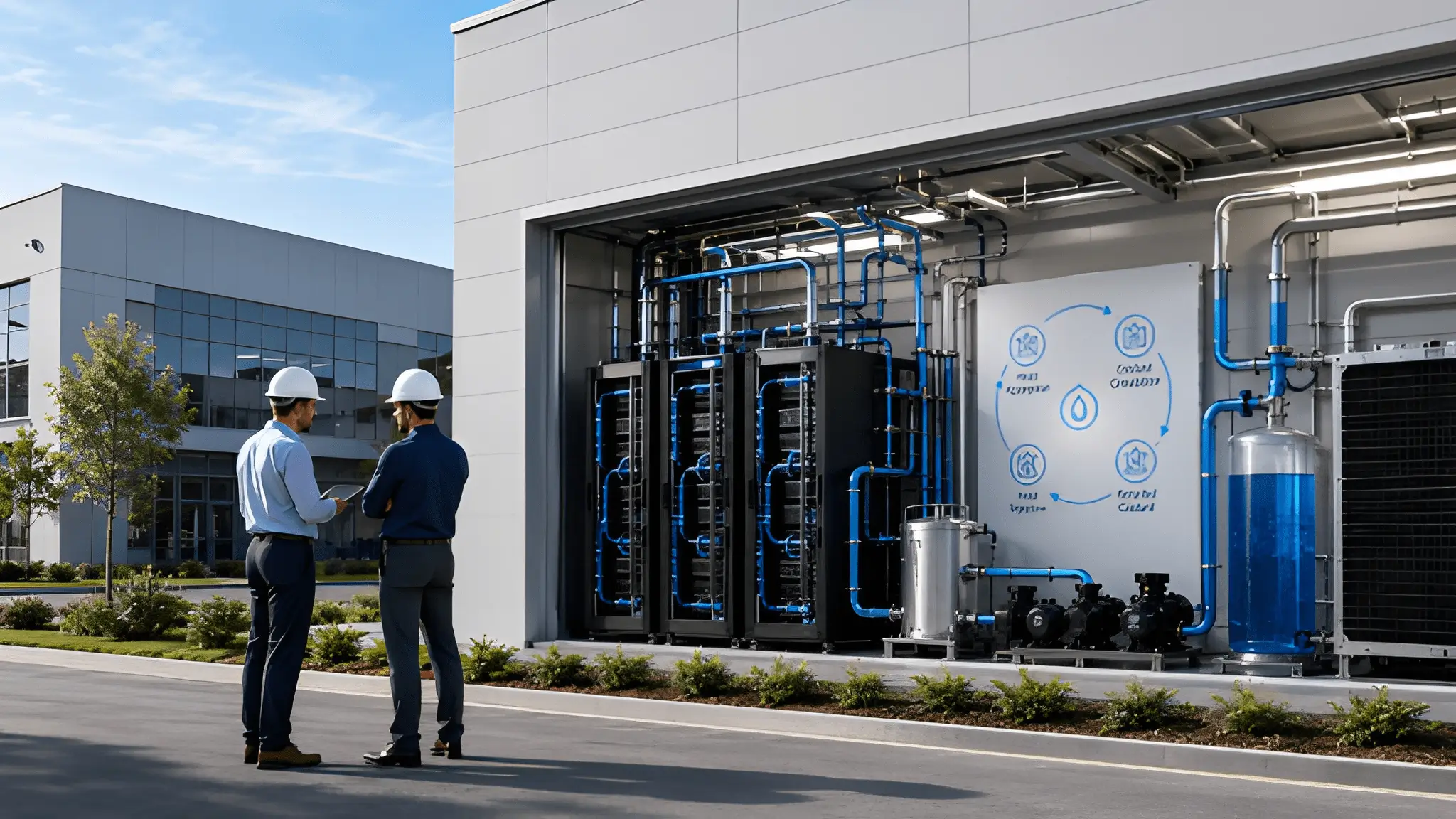
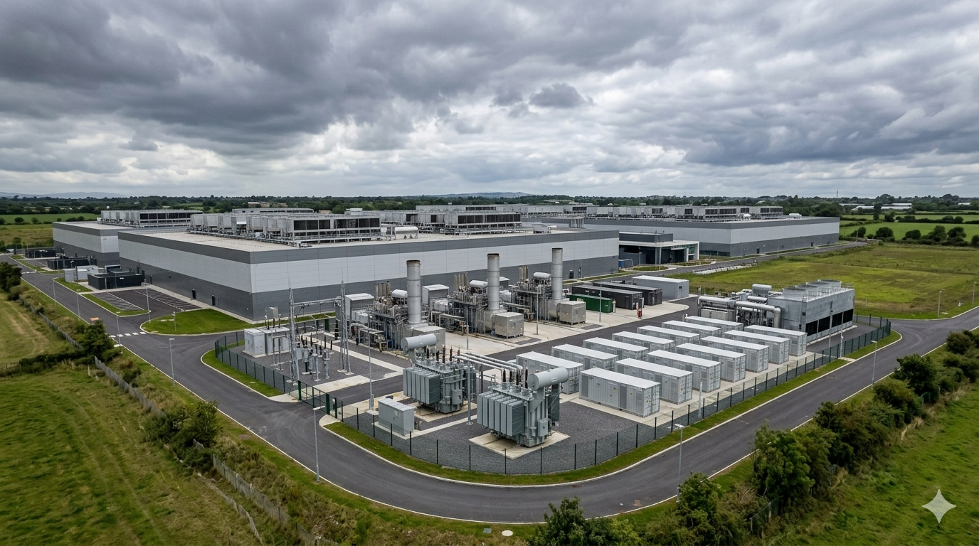
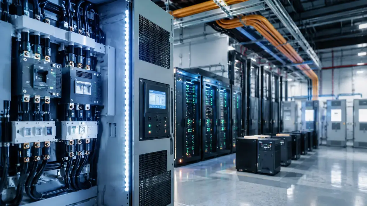
The maturation of chiplet architecture and heterogeneous integration has direct implications for the data center infrastructure that AI compute runs on. Chiplet-based accelerators have different power delivery requirements, different thermal management needs, and different board-level integration requirements than the monolithic designs they replace. Facilities designed around previous generations of AI hardware need to adapt their power distribution, cooling infrastructure, and rack architecture to accommodate the next generation of chiplet-based systems.
The performance trajectory that chiplet architectures enable is also reshaping the infrastructure planning assumptions of the operators procuring AI compute. As memory bandwidth per compute die increases through advanced HBM integration, as die-to-die interconnect bandwidth grows, and as packaging innovation enables denser integration of specialised compute functions, the compute density and memory capacity available in a single rack unit will continue to increase in ways that compound the power and cooling challenges that infrastructure designers are already working to address.
The chiplet transition is not a discrete event but a continuous architectural evolution. Each generation of AI accelerators will integrate more functions into tighter packages, achieve higher memory bandwidth through more advanced HBM generations, and place greater demands on the packaging, cooling, and power delivery infrastructure that enables them to perform at specification. Operators and infrastructure designers who understand this evolution and build adaptability into their facility designs position themselves for the full trajectory of AI compute development. Those who build to the specifications of a single hardware generation limit their ability to keep up.