
The Crisis Nobody at the Utility Substation Can See
The global conversation about AI infrastructure has been almost entirely organised around a single number: gigawatts. How many gigawatts of grid capacity can be secured, how many gigawatts are sitting in interconnection queues, how many gigawatts will be needed by 2030 as training clusters and inference factories multiply across every major market. This framing is accurate and important. Grid-scale power availability is genuinely the binding constraint on data centre deployment in dozens of markets from Northern Virginia to Dublin to Mumbai. The argument for securing gigawatts first is not wrong.
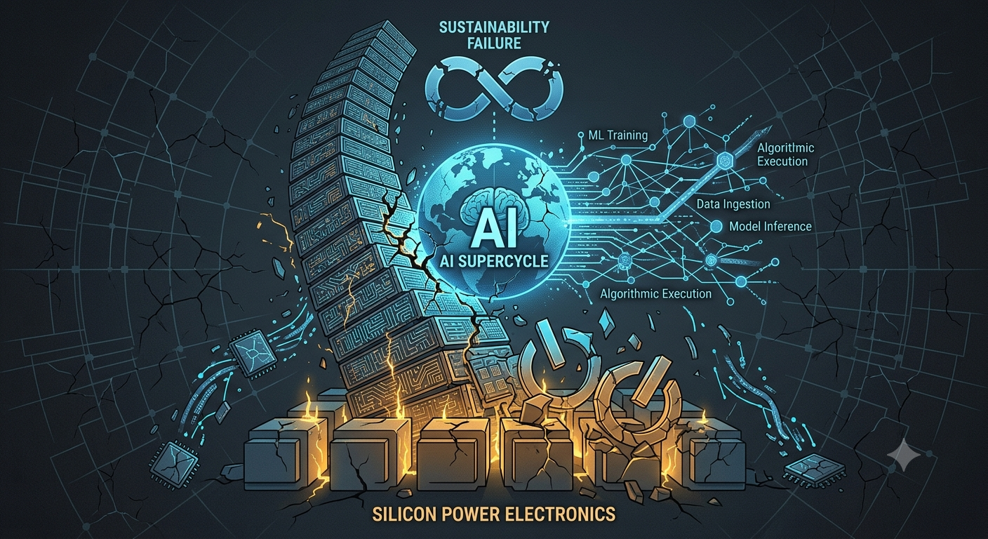
It is, however, incomplete in a way that is becoming financially and operationally consequential as rack power densities push through one hundred and fifty kilowatts toward three hundred, and as GPU thermal design power per chip approaches and in some roadmap projections exceeds two thousand five hundred watts. The bottleneck that grid-level analysis cannot see is the one that exists not at the substation but at the millimetre scale: the last stage of power conversion, in which voltage must be stepped down from the relatively manageable levels at which a data centre can receive and distribute power to the sub-one-volt levels at which a modern AI accelerator die actually operates. This conversion, performed by voltage regulator modules mounted millimetres from the GPU package, is where traditional silicon-based power transistors are running into physical limits that no amount of grid investment can address, and where a structural material science transition, from silicon to wide-bandgap semiconductors, is now in progress with consequences that reach from chip design through data centre architecture to the competitive positioning of an entirely restructured power semiconductor supply chain.
Navitas Semiconductor’s technical documentation on the subject frames the issue with appropriate precision: silicon is at its performance limits for power supply units and will not be able to improve efficiency to meet the needs of AI. This is not a projection about a future state. It is a description of a constraint that is already active and that the power electronics industry is racing to work around, at every stage of the conversion chain, with a different class of semiconductor material, different circuit topologies, and a different set of supplier relationships than the silicon-dominated power electronics ecosystem of the past thirty years produced.
Why Silicon Hits a Wall at the Atomic Level
The Bandgap Problem Is Not Engineering. It Is Physics.
Understanding why silicon cannot solve the power delivery problem that AI-density hardware creates requires engaging with the physics of semiconductor materials rather than the engineering of circuit topologies, because the limitation is not one that can be overcome by redesigning circuit boards or improving manufacturing processes. It is a constraint written into the atomic structure of the material itself.
Silicon has a bandgap of 1.1 electron volts. Bandgap is the energy difference between the valence band, where electrons are bound to atoms, and the conduction band, where they can move freely and conduct electricity. A material with a narrower bandgap conducts electricity more easily, which has historically made silicon excellent for transistors designed to switch between conducting and non-conducting states at high speeds. The same narrow bandgap, however, creates fundamental limitations at three operating conditions that AI data centre power delivery now encounters routinely: high voltage, high temperature, and high switching frequency.
At voltages above approximately six hundred volts, silicon’s narrow bandgap causes electron leakage to become increasingly uncontrollable. The insulating barrier between the conducting state and the non-conducting state in a silicon transistor breaks down at electric field strengths that wide-bandgap materials handle without difficulty. Silicon carbide’s bandgap of 3.3 electron volts and gallium nitride’s 3.4 electron volts, each roughly three times wider than silicon’s, allow these materials to sustain electric fields of three to four times the magnitude that silicon can withstand before breakdown, enabling stable operation at voltages of seventeen hundred volts and above. At the thermal level, silicon’s maximum operating temperature of approximately one hundred and fifty degrees Celsius forces the elaborate cooling systems that add cost and bulk to every silicon-based power conversion stage. SiC conducts heat three times better than silicon, with a thermal conductivity of four hundred and ninety watts per metre-kelvin versus silicon’s one hundred and fifty, maintaining stable electrical characteristics at temperatures that would cause silicon to degrade rapidly. At the switching speed level, silicon’s electron mobility caps practical switching frequencies below one hundred kilohertz. GaN devices, with far higher electron velocity enabled by the two-dimensional electron gas at the GaN heterojunction interface, operate efficiently into the megahertz range, enabling smaller magnetic components and dramatically higher power density per unit volume.
These three limitations, voltage ceiling, thermal bottleneck, and switching speed cap, are not independent problems with independent solutions. They interact. When a silicon-based power converter operates at the high voltage and high current that AI rack densities require, it generates more heat than its thermal management can dissipate efficiently, which degrades its switching performance, which increases its switching losses, which generates more heat. The thirty percent thermal energy loss figure that describes silicon’s performance at AI-scale conversion is not primarily a design inefficiency that better engineering can eliminate. It is the thermodynamic consequence of asking a material operating near its physical limits to perform a conversion task that the material was not structured to execute at that scale.
The Voltage Journey From Grid to GPU Die
Four Stages, Four Failure Points, One Unforgiving Destination
The power conversion challenge at the heart of the AI infrastructure crisis is best understood by tracing the voltage journey that electricity must make from the utility grid to the active region of a GPU die, because the scale of the transformation required is itself the measure of why the problem is so demanding. Utility grid power in a major data centre market arrives at the facility boundary at somewhere between thirteen point eight and thirty-five kilovolts of alternating current. The Rubin Ultra GPU die, at the other end of the journey, operates on a core rail of approximately zero point seven volts of direct current. The voltage must be reduced by a factor of roughly twenty thousand to fifty thousand between these two endpoints, across a power delivery chain that itself consumes a meaningful share of the total power it is handling at each conversion stage.
The Nutty analysis of Nvidia’s 800V partner disclosure at the October 2025 OCP Global Summit articulated the four functional positions of this conversion chain with structural clarity. Front-end conversion takes high-voltage alternating current from the grid and produces a stable high-voltage direct current output, typically the 800V DC bus that Nvidia’s new architecture targets. Eight hundred volt protection circuitry manages hot-swap, fault isolation, and protection functions at the 800V level. Board-level conversion steps the 800V bus down to an intermediate voltage, in current reference designs typically six to twelve volts, that the motherboard and compute tray can distribute efficiently. Point-of-load regulation performs the final step-down from that intermediate voltage to the sub-one-volt level that the GPU core rail requires.
Each of these four positions has its own physical regime, its own material requirements, and its own supplier landscape. The reason that Nvidia disclosed fourteen silicon partners supporting its 800V architecture rather than one or two reflects this four-stage structure: no single semiconductor company and no single material system is optimal for every position in the chain. Front-end conversion at high voltage and relatively lower switching frequency favours silicon carbide. Board-level conversion at higher frequency and intermediate voltage favours gallium nitride. Point-of-load regulation at extremely high current and sub-one-volt output draws on advanced silicon MOSFET technology that wide-bandgap materials do not yet displace on cost grounds at this specific operating point. The transition from silicon to wide-bandgap is therefore not a binary replacement of one material with another. It is a restructuring of a complex multi-stage conversion chain, with different materials advancing at different rates in different positions, and the interactions between stages determining the overall efficiency of the complete path from grid to die.
Nvidia’s 800V Architecture: A Structural Answer to a Structural Problem
Why 54V Could Not Scale to One Megawatt
The decision to announce the 800V high-voltage DC architecture at GTC 2025 was not primarily a technical optimisation. It was an acknowledgement that the prior distribution architecture, built around fifty-four-volt intermediate bus voltage, had reached a physical scaling limit that the trajectory of rack power density had already crossed. The copper problem that Nvidia’s own technical documentation quantifies makes the constraint concrete: delivering one megawatt of power at fifty-four volts requires approximately two hundred kilograms of copper per rack. For a one-gigawatt data centre, that extrapolates to five hundred thousand tonnes of copper, a figure that is not merely impractical but operationally impossible. No data centre can be built on that material basis, and no supply chain can provision copper at that scale for the AI infrastructure buildout that is already in progress.
The physics of power distribution over copper conductors is unambiguous: for a given conductor cross-section, the power that can be transmitted without unacceptable resistive losses is proportional to the square of the voltage. Doubling the distribution voltage from fifty-four to approximately one hundred and ten volts allows roughly four times as much power to be transmitted through the same copper mass. Raising it to eight hundred volts, approximately fifteen times fifty-four, allows the equivalent of two hundred and twenty-five times as much power transmission through the same copper conductor, at equivalent loss levels. A one-megawatt rack that requires two hundred kilograms of copper at fifty-four volts requires approximately nine hundred grams of copper at eight hundred volts. This is the fundamental physical case for high-voltage DC distribution in AI data centres, and it explains why Schneider Electric characterised the shift as physically inevitable in its October 2025 white paper rather than commercially desirable.
The 800V architecture’s system-level efficiency benefits compound on top of the copper reduction. Wolfspeed’s technical analysis of the architecture identified that the 800V DC bus requires 1200V silicon carbide MOSFETs for AC-DC rectification and DC-DC conversion, and that using SiC at this voltage level delivers a twenty-five to forty percent reduction in conversion losses compared to silicon-based equivalents operating at the same voltage. Nvidia’s own documentation cited up to a five percent improvement in end-to-end power efficiency and a seventy percent reduction in maintenance costs from the architectural shift. For a facility drawing hundreds of megawatts of total power, a five percent efficiency improvement is not a marginal gain. It is a reduction in the facility’s annual energy bill measured in tens of millions of dollars, and a commensurate reduction in the cooling infrastructure required to remove the heat that those losses would otherwise generate. The 800V shift is not solving the last-millimetre problem directly, but it is shrinking the total conversion loss budget by addressing the losses that occur at every stage before the last millimetre, leaving more of the total power budget available for the computation that the grid investment was meant to enable.
The Last Millimetre: VRMs, TLVR, and the Final Conversion
Where Physics, Heat, and Speed Collide Simultaneously
The voltage regulator module is not glamorous infrastructure. It does not appear in grid capacity announcements, hyperscaler earnings calls, or data centre campus groundbreaking ceremonies. It is a compact power conversion device mounted millimetres from a GPU package on a server motherboard, and its function is to take whatever intermediate voltage the board-level conversion has delivered, currently typically six to twelve volts in 800V reference designs, and step it down further to the core rail voltage that the GPU die actually operates on, somewhere in the range of zero point seven to one volt depending on the specific device and operating condition. At this final conversion stage, the current levels involved are extraordinary: Nvidia’s Rubin Ultra GPU is projected to draw more than two thousand five hundred watts from a sub-one-volt rail, which implies a current flow at the VRM output of more than two thousand five hundred amps for a single GPU.
Managing two thousand five hundred amps of current flow through a device operating at high switching frequency, in a package that must fit within the physical constraints of a modern server motherboard, within millimetres of a chip that itself generates substantial heat and that imposes strict temperature requirements on all adjacent components, represents a power electronics engineering challenge that is genuinely at the frontier of what semiconductor physics can currently achieve. Texas Instruments’ disclosure at NVIDIA GTC 2026 captured the specific performance achievement that GaN-based VRM technology is delivering at this stage: an 800V to 6V isolated bus converter achieving 97.6% peak efficiency with over two thousand watts per cubic inch of power density, followed by a 6V to sub-1V multiphase buck converter for advanced GPU cores. The efficiency figure is remarkable in absolute terms. A 97.6% efficient converter loses only 2.4% of the power it processes as heat, compared to the approximately thirty percent loss that silicon-based conversion at comparable conversion ratios and power densities produces.
Infineon’s APEC 2026 presentation introduced the TLVR, or trans-inductor voltage regulator, topology in a quad-phase power module specifically engineered for this final conversion stage in AI server applications. The TDM24745T integrates four power stages, a TLVR inductor, and decoupling capacitors in a package measuring just nine by ten by five millimetres, achieving a current density exceeding two amps per square millimetre and a peak current capability of three hundred and twenty amps in that package volume. The TLVR architecture specifically addresses the transient response problem that makes this final stage uniquely demanding: GPU workloads shift rapidly between idle and full load states, creating current transients that a conventional voltage regulator with standard inductor magnetics cannot follow without either allowing the voltage to droop outside the GPU’s tolerance band or storing so much magnetic energy in the inductor that the physical package size becomes incompatible with motherboard geometry. The trans-inductor topology reduces the effective inductance that limits transient response while maintaining the saturation current rating required for sustained full-load operation, a combination that conventional circuit topologies cannot achieve simultaneously.
The Supply Chain Restructuring That Few Investors Have Priced
A Fourteen-Name Partner List and What It Actually Means
When Nvidia disclosed fourteen silicon partners supporting its 800V DC architecture at the OCP Global Summit in October 2025, the announcement generated less financial market attention than any individual GPU product launch typically commands. That misallocation of attention is, in retrospect, a significant analytical error. The fourteen-company list, which included ADI, AOS, EPC, Infineon, Innoscience, MPS, Navitas, onsemi, Power Integrations, Renesas, Richtek, ROHM, STMicroelectronics, and Texas Instruments, describes the restructuring of a power electronics supply chain that collectively serves a market worth approximately thirty-two point eight billion dollars for discrete devices and modules alone, and closer to fifty-seven billion dollars when the broader power management IC layer is included. The partners on this list are not simply supporting a new product. They are being invited into the architectural definition of how every high-density AI data centre built in the next decade will manage power, at every stage of the conversion chain from the utility substation to the GPU die.
Atlas Peak Research’s April 2026 analysis of the global power semiconductor industry identified the strategic split with appropriate precision: broad silicon power remains mature and manufacturing-intensive, automotive and industrial remain the economic centre of gravity, and upstream SiC is in cyclical digestion after the 2019 to 2024 capacity build. Wolfspeed’s bankruptcy and subsequent financial reorganisation through mid-2025 illustrated the capital intensity and risk of the SiC capacity build at the extreme end of the commitment scale. But the same analysis identified the real strategic question as where mix is moving, and the 800V AI data centre architecture is moving the mix toward GaN at the board-level conversion stage and toward SiC at the front-end conversion stage, with silicon maintaining its position primarily at the final point-of-load stage where cost per amp rather than efficiency per watt is the dominant selection criterion.
The investment market’s tendency to evaluate SiC companies through the lens of the electric vehicle cycle, as Atlas Peak noted, has created a structural analytical error that is becoming more costly as the 800V AI data centre architecture defines what the next generation of SiC demand actually looks like. SiC demand grew from approximately three hundred million dollars in 2018 to three point five billion dollars in 2024, roughly twelvefold in six years, driven primarily by the EV traction inverter market. The Moomoo market analysis that Citrini contributed projects AI infrastructure could become half of total SiC demand by 2030, a shift that would mean the AI data centre is absorbing an incremental SiC demand volume approaching or exceeding what the entire EV market currently represents. Companies evaluated as EV cycle plays, which is most of the publicly traded SiC supply chain, are in the process of becoming AI infrastructure plays with the EV revenue as a secondary and potentially declining portion of their addressable market.
The Solid-State Transformer and the Grid-to-Rack Reinvention
Why the Traditional Transformer Has Become the New Bottleneck
The power delivery crisis does not begin at the voltage regulator module. It begins before the power enters the data centre building, at the step-down transformer that converts the medium-voltage grid supply to the voltage levels the facility can distribute internally. Traditional iron-core transformers, the same fundamental technology that has dominated electrical grid infrastructure for more than a century, have become an unexpected chokepoint in the AI data centre buildout for a reason that has nothing to do with their technical adequacy and everything to do with their supply chain: transformer manufacturing is a specialised industry with long lead times, finite production capacity, and an order book that the AI infrastructure boom has overwhelmed to a degree that some analyses characterise as approaching a thirty percent shortage.
Data from the Wolfspeed technical documentation on solid-state transformers cited years-long lead times for the necessary traditional transformers, in a market where data centre expansions in 2025 alone may be responsible for the majority of the supply shortage. A data centre development team that has secured a grid connection, purchased land, finalised facility design, and placed GPU hardware orders can find itself unable to energise its facility because the transformers required to step the grid voltage down to a usable level are simply unavailable within the commercial timeline the project requires. This is not a bottleneck that capital can instantly resolve. Transformer manufacturing has its own material constraints, its own skilled workforce requirements, and its own production facility limitations that respond to demand signals slowly.
The solid-state transformer, enabled specifically by silicon carbide power semiconductors, is the technology response to this bottleneck that is now moving from laboratory demonstration to pilot deployment. A solid-state transformer replaces the iron core and copper windings of a conventional transformer with high-frequency power electronics, performing the same voltage conversion function through rapid switching of SiC transistors rather than through electromagnetic induction at power line frequencies. The result is a device that is substantially smaller and lighter than a conventional transformer of equivalent power rating, that responds faster to load changes, that can be integrated directly with battery storage and DC output stages without additional conversion steps, and that does not have the same manufacturing constraints as conventional transformers because it is built primarily from semiconductor components and standard electronic manufacturing processes.
Wolfspeed’s SST reference design converts high-voltage AC input at the thirteen point eight to thirty-five kilovolt level directly to 800V DC output, eliminating one complete conversion stage from the power chain compared to architectures that use a conventional transformer followed by a separate rectifier. Each eliminated conversion stage is a source of efficiency loss removed, a point of failure removed, and a piece of equipment whose supply chain constraints no longer apply. The STMicroelectronics partnership with Nvidia on 800V HVDC reference designs for data centres, including a twenty-kilowatt eight-level stacked LLC converter using 120V GaN devices on the primary side and achieving operation at 650 kilohertz, represents the board-level equivalent of this same architectural philosophy: fewer stages, higher frequency, smaller magnetics, lower losses, and a conversion topology that only wide-bandgap semiconductors can execute at the switching speeds that make the size and efficiency targets achievable.
The Vertical GaN Breakthrough and What 2026 Established
A Wafer Size Transition That Changed the Cost Equation
The most significant manufacturing milestone in the wide-bandgap semiconductor industry through the first half of 2026 was not a product launch, a new data centre deployment, or a customer announcement. It was a wafer size transition. Infineon Technologies shipped the first 300mm, or twelve-inch, gallium-nitride-on-silicon wafers in 2026, a milestone that represents the transition from the 200mm wafer standard that has defined GaN manufacturing economics for the past decade to the larger wafer format that silicon semiconductor manufacturing has used for its most cost-sensitive, high-volume products for years. This transition matters for a simple reason: a 300mm wafer yields approximately two point two times as many chips as a 200mm wafer of equivalent die size, because the ratio of wafer areas is approximately 2.25. At equivalent process maturity and yield, this means GaN chip costs can approach silicon chip costs at volume, removing the cost premium that has historically made GaN products commercially viable only in applications where their performance advantages justified paying substantially more per device than silicon alternatives required.
The 2026 vertical GaN development that the same analysis flagged as a major trend, in which GaN power transistors are structured vertically through the semiconductor material rather than laterally across its surface, addresses the voltage handling limitation that had previously restricted GaN to applications below approximately six hundred volts. Lateral GaN devices are inherently limited in their voltage capability by the physical constraints of the lateral geometry, which requires very long device structures to handle high voltages and consequently compromises power density. Vertical GaN devices stack the active device structures through the thickness of the semiconductor material, enabling the same voltage blocking that has historically been SiC’s exclusive domain to be achieved in GaN material with GaN’s superior switching speed characteristics. The 2026 vertical GaN breakthrough allowing the technology to handle 1200V and above, the voltage rating required for the front-end conversion stage of the 800V data centre architecture, creates the first genuinely competitive alternative to SiC at the highest-voltage positions in the power conversion chain.
The Wolfspeed restructuring, which emerged from its financial reorganisation as a leaner 200mm-focused manufacturer with a more sustainable capital structure, illustrates the competitive pressure that GaN’s cost trajectory is creating at the SiC layer. SiC maintains its advantages over GaN in thermal conductivity and maximum operating temperature, which remain relevant for the most thermally stressed applications. But the gap in switching efficiency, power density per unit volume, and now manufacturing cost is narrowing with each generation of GaN process maturation, creating competitive pressure at the specific performance envelope where the two materials overlap and where AI data centre power conversion requirements sit. The IDTechEx power electronics market analysis that specifically benchmarks silicon, SiC, GaN, and ultra-wide bandgap materials including diamond, gallium oxide, and aluminium nitride in the data centre context reflects the industry’s recognition that the material choice at each stage of the conversion chain is no longer a binary silicon-versus-other question but a nuanced optimisation across a growing landscape of competing semiconductor technologies.
What the Efficiency Numbers Actually Mean at Gigawatt Scale
Compounding the Loss Budget Across an Entire AI Infrastructure Cycle
The efficiency claims associated with wide-bandgap semiconductor power conversion deserve to be examined at the system scale that the AI infrastructure buildout actually operates at, because the difference between a ninety-seven percent efficient conversion stage and an eighty-seven percent efficient silicon-based alternative is not a marginal improvement when multiplied across gigawatts of total power draw. At the chip level, every watt that power conversion loses to heat is a watt that does not reach the GPU die and perform computation. At the facility level, every watt of conversion loss generates heat that the cooling system must remove, consuming additional power in doing so. At the grid level, every watt of conversion loss is a watt that must be generated, transmitted, and supplied to the data centre above what the computation itself requires, contributing to the grid capacity constraints that the AI infrastructure conversation treats as an external supply problem rather than a partially internal efficiency problem.
A facility drawing three hundred megawatts of grid power to run a Vera Rubin cluster at the Blackwell-era thirty percent silicon conversion loss rate loses approximately ninety megawatts to heat across the conversion chain before any of that power reaches a GPU die. At a silicon carbide and GaN-enabled ten percent total conversion loss rate across the same chain, the same facility loses thirty megawatts. The sixty-megawatt difference is not simply an efficiency statistic. It is sixty megawatts of grid-connected capacity that does not need to be built, sixty megawatts of cooling capacity that does not need to be installed, sixty megawatts of power purchase agreement volume that does not need to be contracted, and sixty megawatts of carbon emissions at the marginal generation mix that does not need to be offset. At a thousand-megawatt gigafactory scale, the efficiency improvement translates to six hundred megawatts of avoided infrastructure, a figure that exceeds the total data centre capacity of multiple entire European countries operating in the current environment.
This is the system-level consequence of the last-millimetre problem that grid-focused AI infrastructure analysis misses entirely. The battle for gigawatts at the substation is real and consequential. The battle for efficiency percentage points at the voltage regulator module is equally real and equally consequential, and it is being decided by semiconductor material properties and circuit topologies that most AI infrastructure commentary treats as engineering details rather than strategic variables. The fourteen companies on Nvidia’s 800V partner list are not implementing a customer preference. They are defining the efficiency boundary that determines how much of the world’s grid investment in AI infrastructure actually reaches a GPU die and produces computation, versus how much of it dissipates as heat in a conversion stage that silicon’s physical structure could never have been expected to sustain at the scale the AI supercycle demands.
The Infrastructure Transition Nobody Named as a Transition
The AI infrastructure supercycle has been narrated as a story about chips, data centres, and power grids. The actual story, viewed from the millimetre scale rather than the gigawatt scale, is a story about materials science: a structural transition from silicon to wide-bandgap semiconductors at every stage of the power conversion chain, driven by the physical impossibility of delivering two-thousand-five-hundred-watt GPU core power at sub-one-volt rails through transistors operating at their thermal and electrical breakdown limits. Silicon did not fail to serve the AI industry. It reached its physical ceiling exactly as the AI industry was demanding performance levels that no incremental silicon process improvement could have accommodated.
GaN and SiC are not displacing silicon because they are incrementally better materials. They are displacing it because they are physically different at the atomic structure level in the specific ways that the last-millimetre power delivery problem requires: wider bandgap for higher voltage tolerance, better thermal conductivity for operation in the heat-saturated environment adjacent to a kilowatt-class GPU, and higher electron mobility for the megahertz-range switching speeds that enable the magnetics miniaturisation that AI server power density demands. The fourteen-company 800V ecosystem that Nvidia has assembled, and the fourteen-company equivalent that every major GPU vendor will assemble as it follows the same architectural inevitability, represents the supply chain infrastructure of this transition, built at the pace and scale the AI supercycle has imposed rather than the pace and scale that a conventional technology generation transition would have allowed.
The last millimetre, the conversion stage between the six-volt intermediate bus and the zero-point-seven-volt GPU core rail, is where the entire power delivery investment from the utility substation either delivers usable computation or disappears as heat. Getting it right, in material selection and circuit topology and package integration, is not a detail of data centre engineering. It is the final determinant of how much of the world’s AI infrastructure investment actually reaches a GPU die and produces the intelligence the supercycle was built to generate.


